System and method for determining substrate doping density in metal oxide semiconductor devices

a semiconductor device and substrate technology, applied in semiconductor/solid-state device testing/measurement, instruments, specific gravity measurement, etc., can solve the problems of destroying the ecv method, inconvenient and inaccurate kleinknecht method for mosfet devices, and bound to create erroneous sub>s, etc., to achieve the precise value of the substrate doping density na

Active Publication Date: 2009-03-31
NAT SEMICON CORP
View PDF3 Cites 3 Cited by
  • Summary
  • Abstract
  • Description
  • Claims
  • Application Information

AI Technical Summary

Problems solved by technology

However, the ECV method is destructive because it etches a hole in the semiconductor sample.
However, the Kleinknecht method is inconvenient and inaccurate for MOSFET devices.
The prior art methods that determine the value of the substrate doping density Na by assuming a constant value for the surface potential φS are bound to create erroneous results.

Method used


Image

  • System and method for determining substrate doping density in metal oxide semiconductor devices
  • System and method for determining substrate doping density in metal oxide semiconductor devices
  • System and method for determining substrate doping density in metal oxide semiconductor devices

Examples


Embodiment Construction

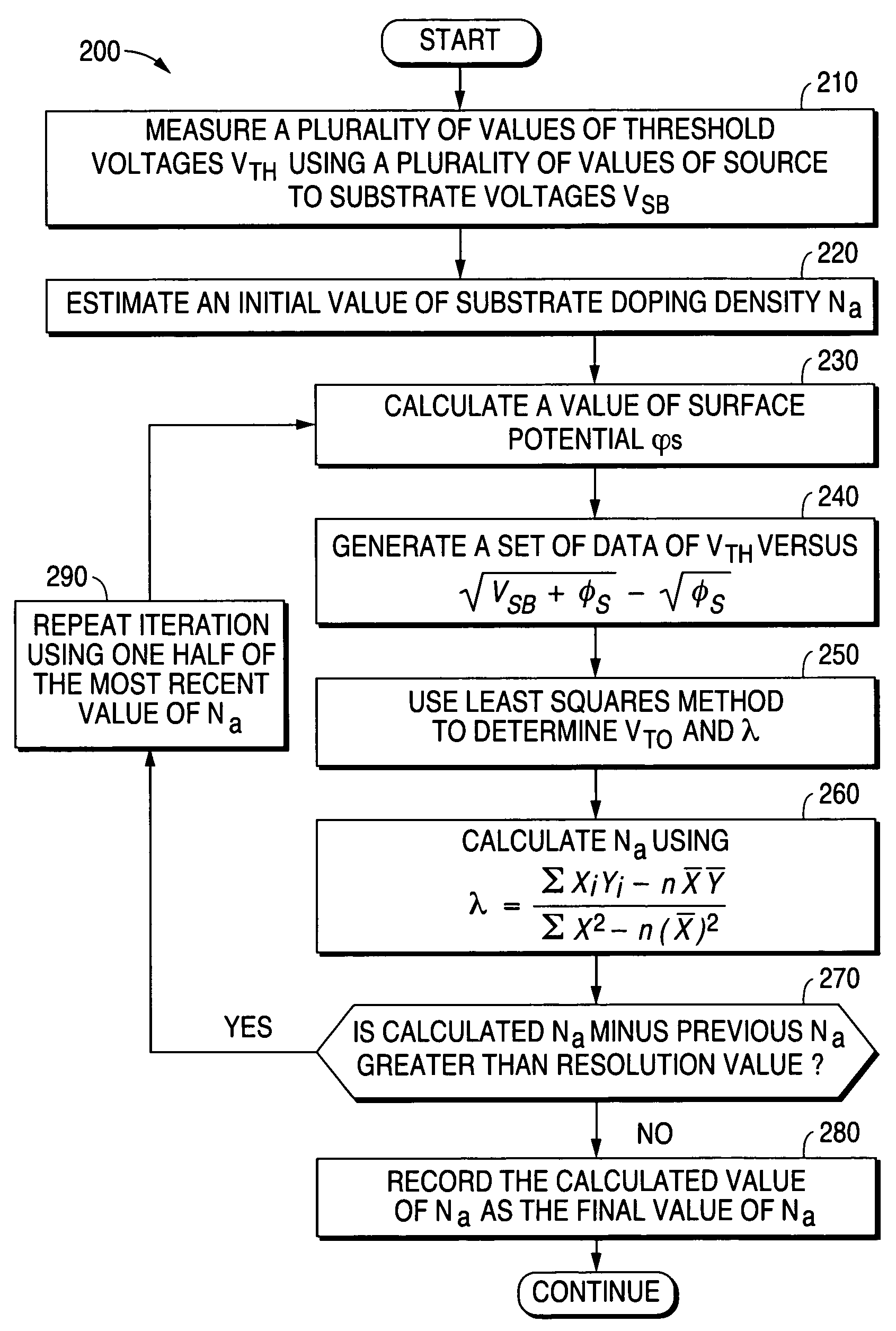
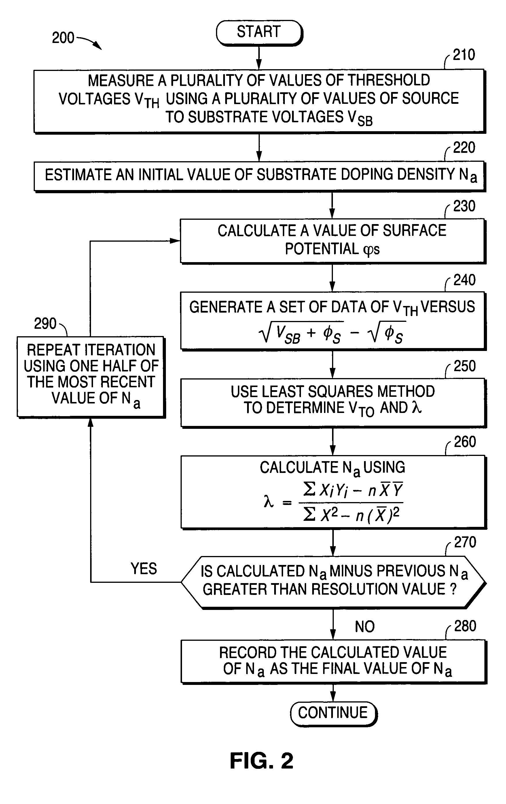
[0035]FIGS. 1 through 3, discussed below, and the various embodiments used to describe the principles of the present invention in this patent document are by way of illustration only and should not be construed in any way to limit the scope of the invention. Those skilled in the art will understand that the principles of the present invention may be implemented with any type of suitably arranged metal oxide semiconductor field effect transistor (MOSFET) device.

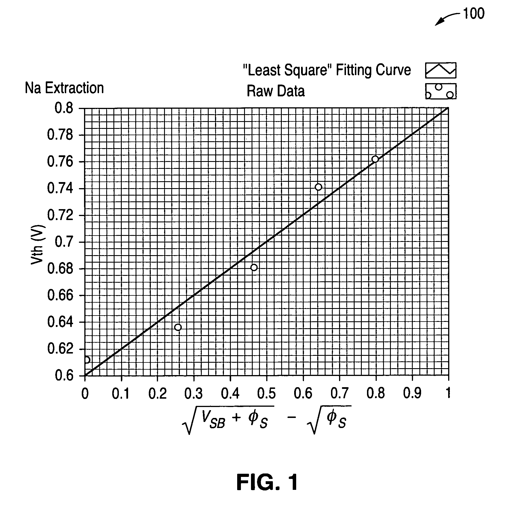
[0036]As previously mentioned, the prior art approach assumes that the value of the surface potential φS is constant. This assumption of the prior art simplifies the calculation by making it easier to solve Equation (1). For convenient reference, Equation (1) is

VTH=VTO+λ(√{square root over (VSB+φS)}−√{square root over (φS)})  Eq. (1)

[0037]However, this simplifying assumption also decreases the precision with which the value of the substrate doping density Na can be calculated. As will be more fully described below, the method ...


PUM

PropertyMeasurementUnit
threshold voltage VTOaaaaaaaaaa
doping densityaaaaaaaaaa
threshold voltageaaaaaaaaaa

Abstract

A system and method are disclosed for very accurately determining a value of a substrate doping density in a metal oxide semiconductor device. A plurality of values of threshold voltage of a device under test are measured using a plurality of different values of source to substrate bias voltage. Then a linear relationship is determined between the plurality of values of threshold voltage and a plurality of different values of an expression that is a function of the source to substrate bias voltage and a function of a surface potential of the device. A very accurate value of the substrate doping density is reiteratively calculated from the linear relationship without assuming that the surface potential of the device has a constant value.

Description

TECHNICAL FIELD OF THE INVENTION[0001]The present invention is generally directed to the manufacture of integrated circuits and, in particular, to a system and method for determining with high precision a substrate doping density in metal oxide semiconductor (MOS) devices.BACKGROUND OF THE INVENTION[0002]A metal oxide semiconductor field effect transistor (MOSFET) device is a semiconductor device in which a gate dielectric layer electrically insulates a channel region of a semiconductor body from an overlying gate electrode. The channel region extends between a source region and a drain region of the transistor. The substrate region or the substrate (sometimes referred to as the body) is manufactured having an opposite conductivity type than the source and drain.[0003]The charge carriers for an n-channel MOSFET are electrons. The charge carriers for a p-channel MOSFET are holes. The charge carriers move from the source region through the channel region to the drain region when appro...

Claims


Application Information

Patent Timeline
Patent Type & Authority Patents(United States)
IPC IPC(8): G01N31/00G01N9/36G06F15/00G06F19/00
CPCH01L22/14
Inventor BU, JIANKANGBELCHER, WILLIAM S.
Owner NAT SEMICON CORP
Why Eureka
Try Eureka