Multiplier array processing system with enhanced utilization at lower precision

a processing system and multiplier array technology, applied in the direction of computation using denominational number representation, memory adressing/allocation/relocation, instruments, etc., can solve the problem of not appreciably changing the relation between the size of the operand, affecting the utilization rate of the multiplier and the adder array resources, and consuming greater circuit resources for high-precision operations. , to achieve the effect of improving the utilization rate of the multiplier and reducing the utilization rate of the adder array

Inactive Publication Date: 2009-03-24
MICROUNITY
View PDF127 Cites 70 Cited by
  • Summary
  • Abstract
  • Description
  • Claims
  • Application Information

AI Technical Summary

Benefits of technology

[0010]The present invention relates to a method, instruction, and system which improves the utilization of a multiplier and adder array for performing multiply and add operations at a lower precision than the full word size of the processor and particularly the multiplier and adder array.
[0011]In accordance with an exemplary embodiment of the present invention, a novel group-multiply-and-sum instruction is performed wherein operands which are the word size of the processor, for example, 128-bits, are divided into symbols where the symbols are 64, 32, 16, 8, 4, 2, or 1 bit. Multiplier and multiplicand symbols are then multiplied together, and the products are added together so as to produce a single scalar result. The instruction performs twice as many multiplies as a group-multiply-and-add instruction (as described in related U.S. patent application Ser. No. 08 / 516,036, hereinafter referred to as the parent application) of the same symbol size. The instruction also avoids fixed-point overflows, because in the current example, the 128-bit result is large enough to hold the sum.
[0016]As described in detail below, the present invention provides important advantages over the prior art. Most importantly, the present invention optimizes both system performance and overall power efficiency. The present invention performs a greater number of multiply operations and add operations in a single instruction without increasing the size of the result of this single instruction. The present invention arranges these operations in a manner which is advantageous both for implementation of digital signal processing algorithms, as the instructions perform these operations with greater parallelism and greater avoidance of arithmetic overflow, and which is advantageous for implementation of the multiplier itself, as these multipliers are formed from a partitioning of a single multiplier array, thereby overcoming significant disadvantages suffered by prior art devices as detailed above.

Problems solved by technology

High-precision operations generally consume greater circuit resources than low-precision operations.
These techniques can reduce the size of multiplier arrays and reduce the delay of addition arrays, however, these techniques do not appreciably change the relation between the size of the operand and the size of the multiplier and adder arrays.
Thus, while this technique produces results with the same number of bits as the 64-bit product, decreasing the symbol size results in a proportionately decreasing utilization of the multiplier and adder array resources.
Clearly, a design that has sufficient resources for a 64-bit multiply will be under-utilized for multiplies on smaller symbols.

Method used


Image

  • Multiplier array processing system with enhanced utilization at lower precision
  • Multiplier array processing system with enhanced utilization at lower precision
  • Multiplier array processing system with enhanced utilization at lower precision

Examples


Embodiment Construction

[0031]A multiplier array processing system is described wherein numerous specific details are set forth, such as word size, data path size, and instruction formats etc., in order to provide a thorough understanding of the present invention. It will be obvious, however, to one skilled in the art that these specific details need not be employed to practice the present invention. In other instances, well known processor control path and data path structures have not been described in detail in order to avoid unnecessarily obscuring the present invention.

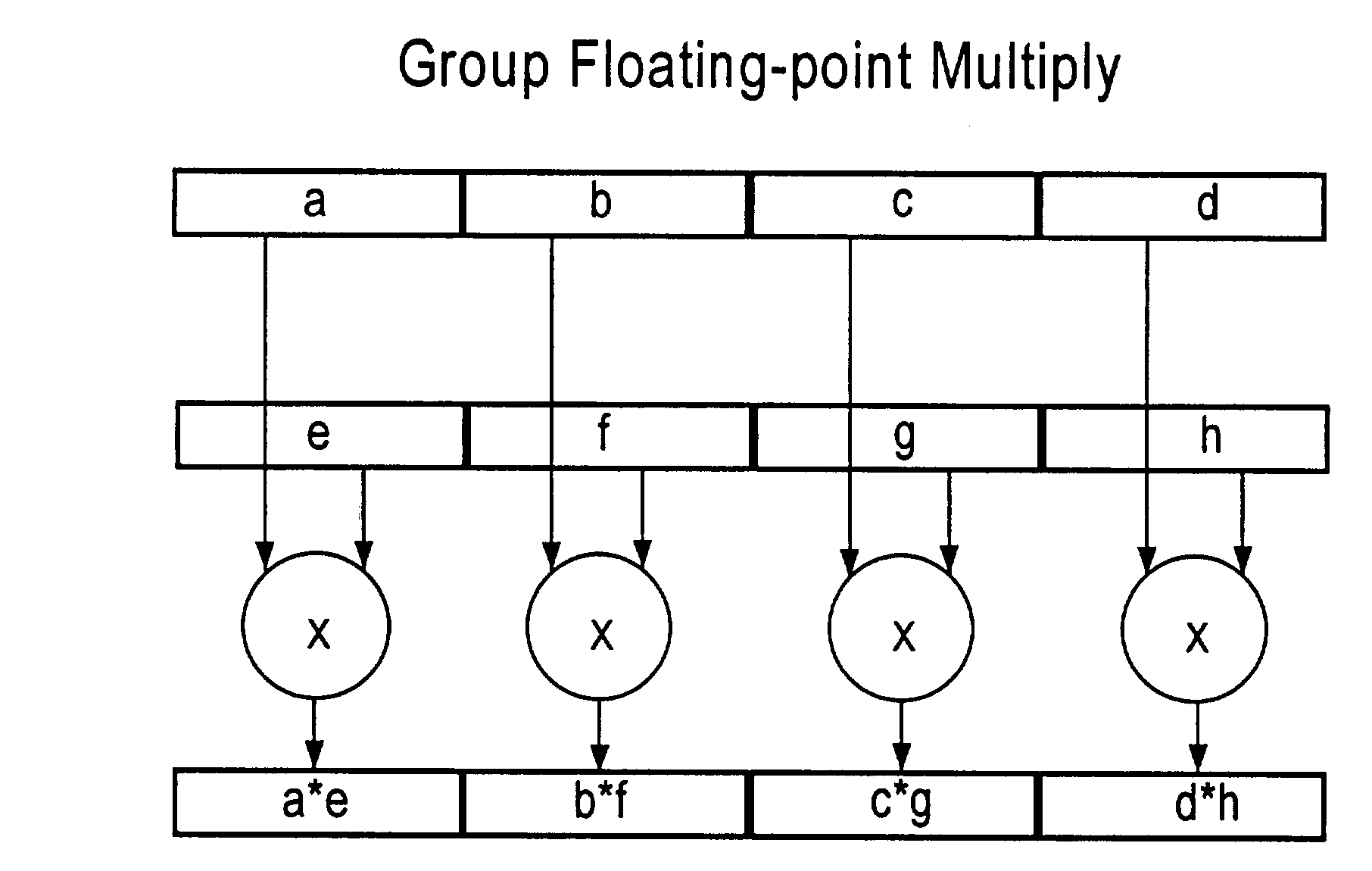
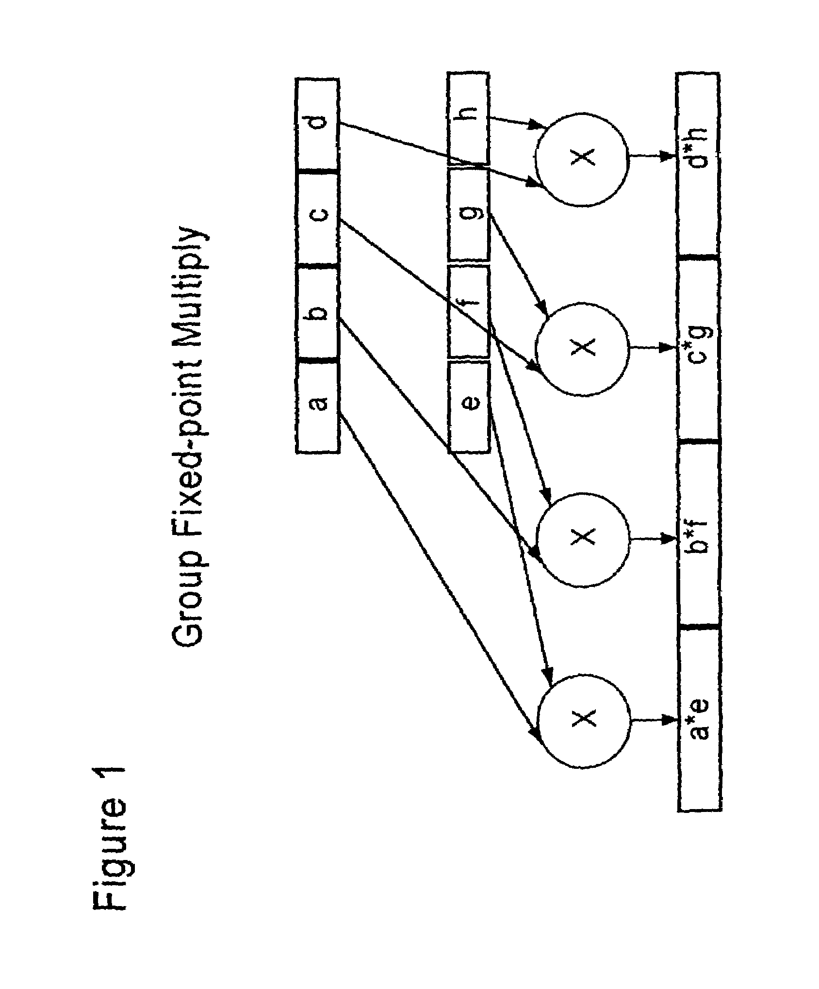
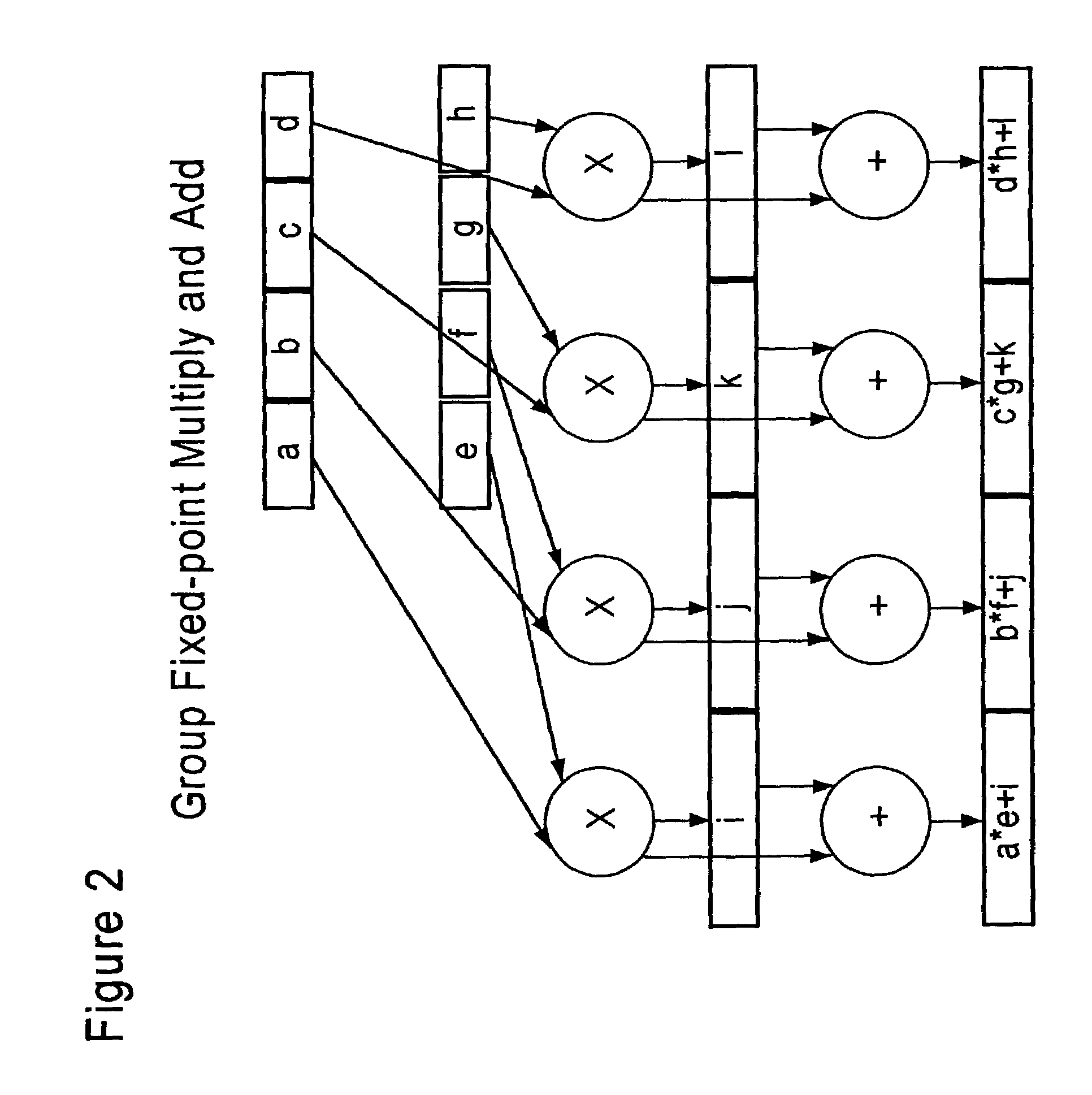
[0032]FIGS. 1-4 illustrate instructions from the instruction set forth in the parent application Ser. No. 08 / 516,036 filed Aug. 16, 1995.

[0033]FIGS. 1 and 2 relate to fixed-point multiplication instructions, wherein groups of symbols of 64-bit total size are multiplied together, thereby producing groups of products of 128-bit total size. The individual symbols are of sizes from 1 bit to 64 bits, i.e., 64×1-bit, 32×2-bit, 16×4-bit, 8×8-b...


PUM


Abstract

A multiplier array processing system which improves the utilization of the multiplier and adder array for lower-precision arithmetic is described. New instructions are defined which provide for the deployment of additional multiply and add operations as a result of a single instruction, and for the deployment of greater multiply and add operands as the symbol size is decreased.

Description

RELATED APPLICATIONS[0001]This application is a continuation of application Ser. No. 09 / 377,182, filed Aug. 19, 1999, now U.S. Pat. No. 6,584,482, which is a continuation of Ser. No. 08 / 857,596, filed May 16, 1997, now U.S. Pat. No. 5,953,241, which claims priority to Provisional Application Ser. No. 60 / 021,132, filed May 17, 1996, and also is a Continuation-in-Part of application Ser. No. 08 / 516,036, filed Aug. 16, 1995, now U.S. Pat. No. 5,742,840.FIELD OF THE INVENTION[0002]The present invention relates to an instruction set and data paths of processors which perform fixed-point and floating-point multiply and add operations, and particularly processors which perform both multiply and add operations as a result of a single instruction.BACKGROUND OF THE INVENTION[0003]A general-purpose processing system which performs multiply and add operations may allow these arithmetic operations to be performed at varying precision. High-precision operations generally consume greater circuit r...

Claims


Application Information

Patent Timeline
IPC IPC(8): G06F7/50G06F7/52G06F9/30G06F9/302G06F9/38G06F12/08G06F12/10G06F15/78H04N21/2365H04N21/238H04N21/434
CPCG06F9/30G06F9/30018G06F9/30025G06F9/30032G06F9/30036G06F9/30043G06F9/30145G06F9/3802G06F9/3867G06F9/3869G06F15/7832G06F15/7842H04N21/2365H04N21/238H04N21/23805H04N21/4347G06F7/5443G06F9/30014Y02B60/1225G06F7/483G06F2207/382G06F2207/3828Y02D10/00
Inventor HANSEN, CRAIG C.
Owner MICROUNITY
Why Eureka
Try Eureka