
Modification of electrical properties of display cells for improving electrophoretic display performance

a technology of display cells and electrical properties, applied in the direction of instruments, non-metal conductors, conductors, etc., can solve the problems of resistivity of adhesives, inferior image contrast and bistability of display cells, and degraded image bistability, so as to improve the performance of electrophoretic displays, increase switching rate and image bistability, and reduce reverse bias

Active Publication Date: 2009-03-17
E INK CORPORATION
View PDF31 Cites 62 Cited by
  • Summary
  • Abstract
  • Description
  • Claims
  • Application Information

AI Technical Summary

Benefits of technology

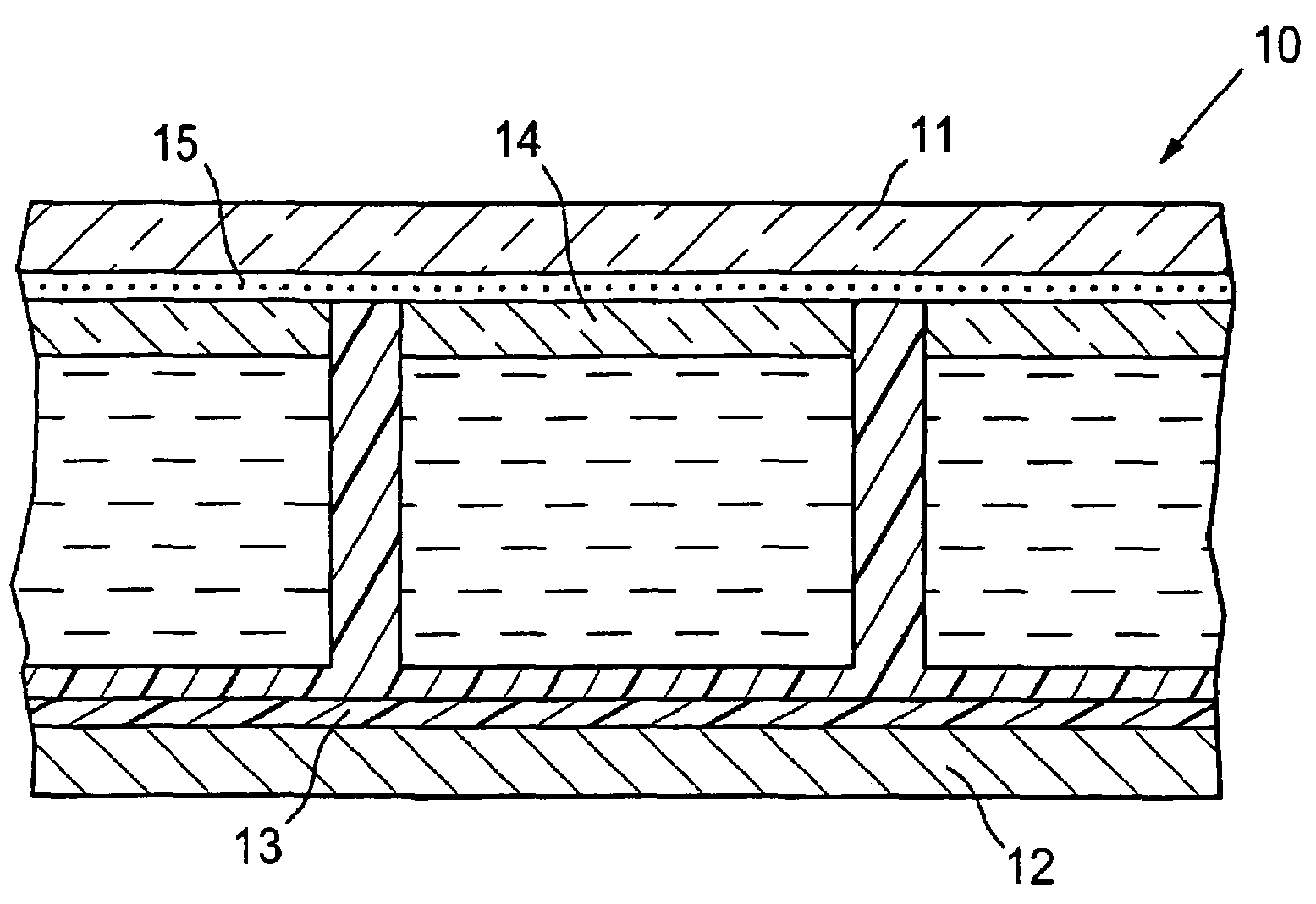
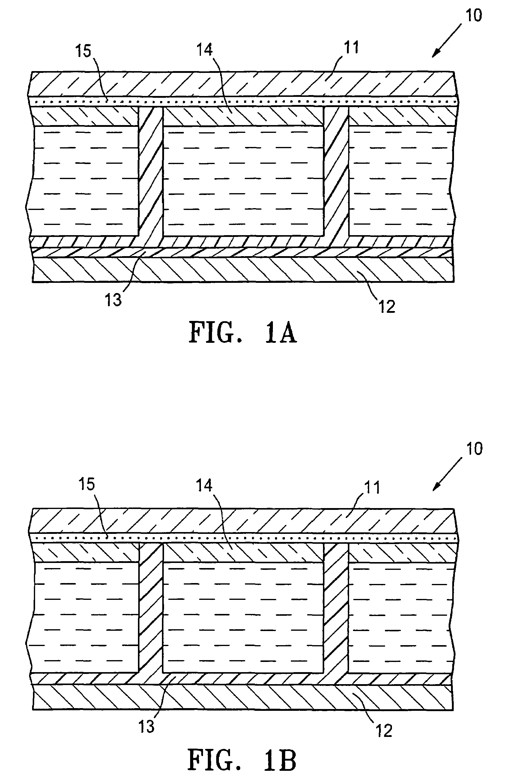
[0012]The present invention relates to compositions and methods for improving the performance of an electrophoretic display. More specifically, it has been found that the performance of an electrophoretic display may be improved by incorporating a conductive filler having a volume resistivity of less than about 104 ohm cm, preferably about 102 to about 103 ohm cm, into a composition for the formation of display cells. In other words, it has been found that the display cells having an intended volume resistivity of about 107 to 1010 ohm cm may be achieved by blending a conductive filler having a volume resistivity of less than about 104 ohm cm, preferably about 102 to about 103 ohm cm, into a display cell composition.
[0015]The second aspect of the invention is directed to a method for improving the performance of an electrophoretic display which method comprises adding a conductive filler in the form of nanoparticles and having a volume resistivity of less than about 104 ohm cm, preferably about 102 to about 103 ohm cm, into a composition for the formation of display cells.
[0016]The third aspect of the invention is directed to a method for improving the performance of an electrophoretic display which method comprises adding a conductive filler in the form of nanoparticles and having a volume resistivity of less than about 104 ohm cm, preferably about 102 to about 103 ohm cm, into both a composition for the formation of display cells and a composition for the formation of a dielectric layer.
[0019]The sixth aspect of the present invention is directed to a method for improving the performance of an electrophoretic display by incorporating non-light-absorbing conducting particles into a composition for the formation of display cells.
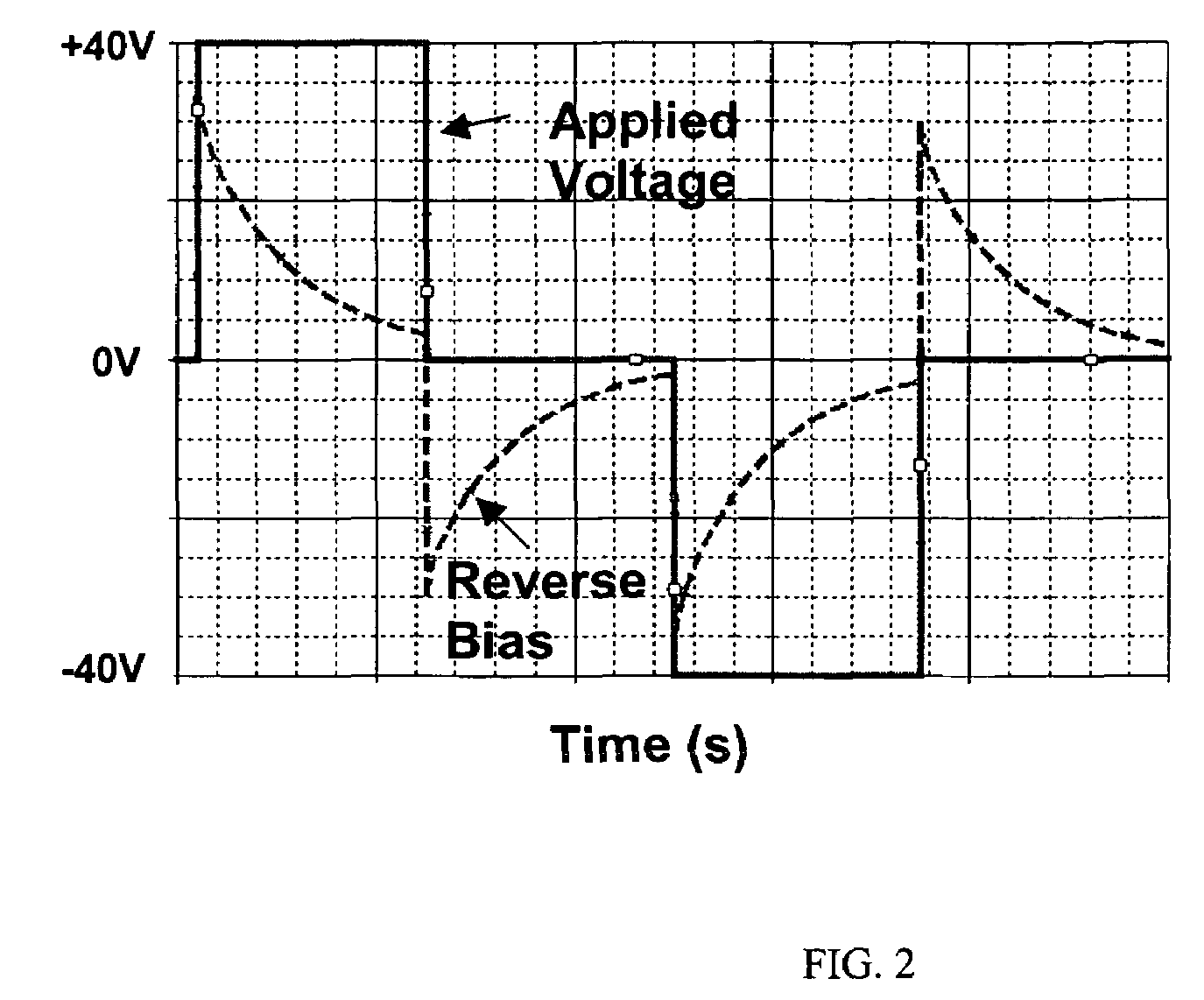
[0020]The electrophoretic display prepared from the present invention shows an increase in switching rate and image bistability even at low driving voltages without trade-off in display longevity and image uniformity. In addition, for the microcup-based electrophoretic displays, no detrimental effect on the embossing shim or the structure integrity of the resulting microcups is observed when the conductive nanoparticles are incorporated into the composition for the formation of the microcups. The reverse bias may also be reduced significantly without tradeoff in the image uniformity or switching performance.
[0021]Furthermore, by optimizing the electrical properties of the display cells, the process window for the roll-to-roll manufacturing is also widened, with high yields. This is possible because the requirement for the bottom thickness of the display cells is more relaxed.

Problems solved by technology

However in certain cases, the image bistability may degrade due to reverse bias.
As a result, the display would have inferior image contrast and bistability.
U.S. Pat. No. 6,657,772 discloses that the volume resistivity of an adhesive layer can be decreased by blending a conductive filler into the adhesive composition, however, it also acknowledges that there are great difficulties in adopting this approach to achieve the volume resistivity of about 1010 ohm cm required for an adhesive layer used in an electrophoretic display.
Most conductive fillers are not transparent and require tedious grinding or milling to be uniformly dispersed into the display cell structure or other dielectric layers.
Aggregation of the filler particles may results in undesirable effects such as poor image uniformity, mottling or sometimes short circuit of the display.
In the case of microcup-based EPDs, incorporation of conductive filler particles into the microcup structure or the top-sealing and / or adhesive layer tends to cause problems in the manufacture of the microcups.
Defective microcups may be resulted from insufficient or non-uniform degree of photoexposure during a microcup forming process (e.g., microembossing or photolithographic exposure).
Moreover, if the particle size of the filler particles is relatively large as compared with the degree of surface roughness or thickness of the layer comprising the particles, damage on the embossing shim or the conductor film such as ITO / PET during embossing may be observed, particularly when the hardness of the conductive filler is higher than that of the shim material or conductor film used.

Method used


Image

  • Modification of electrical properties of display cells for improving electrophoretic display performance
  • Modification of electrical properties of display cells for improving electrophoretic display performance
  • Modification of electrical properties of display cells for improving electrophoretic display performance

Examples


examples

[0065]The following examples are given to enable those skilled in the art to more clearly understand and to practice the present invention. They should not be considered as limiting the scope of the invention, but merely as being illustrative and representative thereof.

preparation 1

Synthesis of a Reactive Protective Colloid Rf-Amine

[0066]

[0067]17.8 Gm of Krytox® methyl ester (DuPont, MW=about 1780, g=about 10) was dissolved in a solvent mixture containing 12 gm of 1,1,2-trichlorotrifluoroethane (Aldrich) and 1.5 gm of α,α,α-trifluorotoluene (Aldrich). The resultant solution was added drop by drop into a solution containing 7.3 gm of tris(2-aminoethyl)amine (Aldrich) in 25 gm of α,α,α-trifluorotoluene and 30 gm of 1,1,2-trichlorotrifluoroethane over 2 hours with stirring at room temperature. The mixture was then stirred for another 8 hours to allow the reaction to complete. The IR spectrum of the crude product clearly indicated the disappearance of C═O vibration for the methyl ester at 1780 cm−1 and the appearance of C═O vibration for the amide product at 1695 cm−1. Solvents were removed by rotary evaporation followed by vacuum stripping at 100° C. for 4-6 hours. The crude product was then dissolved in 50 ml of the PFS2 solvent (perfluoropolyether from Solvay S...

preparation 2

Preparation of Electrophoretic Fluid

[0069]8.93 Gm of Desmodur® N3400 aliphatic polyisocyanate (from Bayer AG) was dissolved in 4.75 gm of acetone (99.9%, from Burdick & Jackson) and homogenized for 10 seconds with a rotor-stator homogenizer (IKA ULTRA-TURRAX T25, IKA WORKS) at ambient temperature. To the resultant solution, 13.61 gm of TiO2 (R706, from DuPont) was added and homogenized for 2 minutes. To the resultant TiO2 dispersion, a solution containing 1.42 gm of 1,5-pentanediol (BASF), 0.30 gm of triethanolamine (99%, Dow), 2.75 gm of polypropylene oxide (MW=725, from Aldrich) and 1.25 gm of acetone was added and homogenized for 30 seconds. 0.37 Gm of a 2% dibutyltin dilaurate (Aldrich) solution in acetone was then added and homogenized for 1 minute and 30 seconds. In the final step, 50.0 gm of HT-200 (Solvay Solexis) containing 2.25 gm of Rf-amine4900 (prepared according to Preparation 1 above) was added and homogenized for 4 minutes. The resultant microparticle dispersion was ...


PUM

PropertyMeasurementUnit
volume resistivityaaaaaaaaaa
particle sizeaaaaaaaaaa

Abstract

The invention is directed to a method for improving the performance of electrophoretic displays by modifying the electrical properties of the display cells.

Description

RELATED APPLICATION[0001]This application claims the priorities under 35 USC 119(e) of U.S. Provisional Application No. 60 / 547,317 filed on Feb. 23, 2004. The whole content of the priority application is incorporated herein by reference in its entirety.BACKGROUND OF THE INVENTION[0002]1. Field of the Invention[0003]The invention is directed to compositions and methods for improving the performance of electrophoretic displays by modifying the electrical properties of the display cells.[0004]2. Description of Related Art[0005]The electrophoretic display (EPD) is a non-emissive device based on the electrophoresis phenomenon of charged pigment particles suspended in a solvent. It was first proposed in 1969. The display usually comprises two plates with electrodes placed opposing each other, separated by spacers. One of the electrodes is usually transparent. An electrophoretic fluid composed of a colored solvent with charged pigment particles dispersed therein is enclosed between the two...

Claims


Application Information

Patent Timeline
Patent Type & Authority Patents(United States)
IPC IPC(8): H01B1/20G02B26/00G02F1/167G02F1/16756H01C1/00
CPCG02F1/167G02F1/16756
Inventor WENG, XINCHEN, YAJUANTSENG, SCOTT C-JHOU, JACK
Owner E INK CORPORATION
Learn More