
Package for high frequency waves containing high frequency electronic circuit

a technology of electronic circuits and high frequency waves, applied in the direction of waveguide devices, basic electric elements, semiconductor devices, etc., can solve the problems of large ohm loss, ineffective transmission of applied voltage, and inability to obtain a sufficient current capacity, so as to achieve the effect of raising the current capacity

Active Publication Date: 2009-02-03
KK TOSHIBA
View PDF11 Cites 20 Cited by
  • Summary
  • Abstract
  • Description
  • Claims
  • Application Information

AI Technical Summary

Benefits of technology

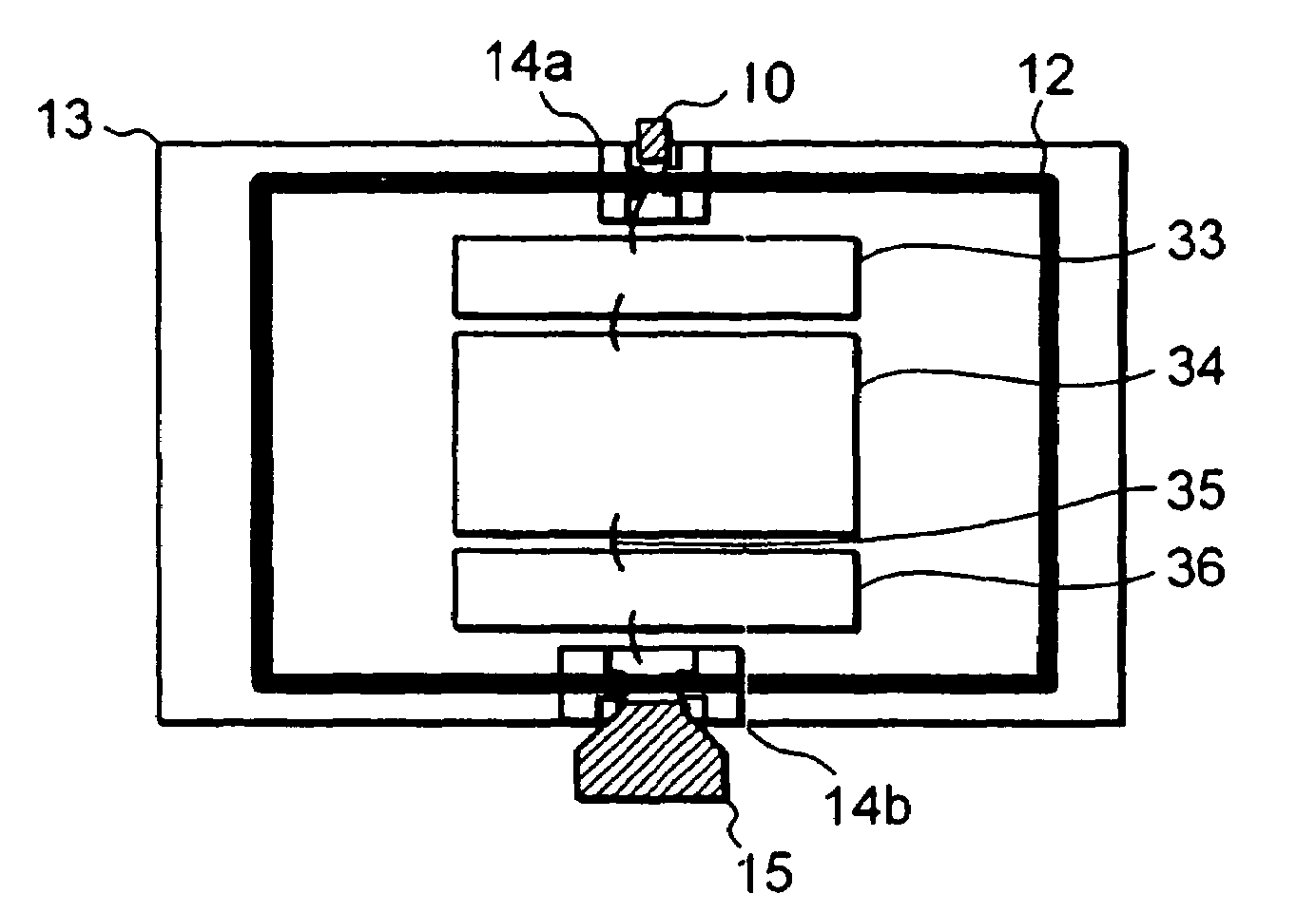
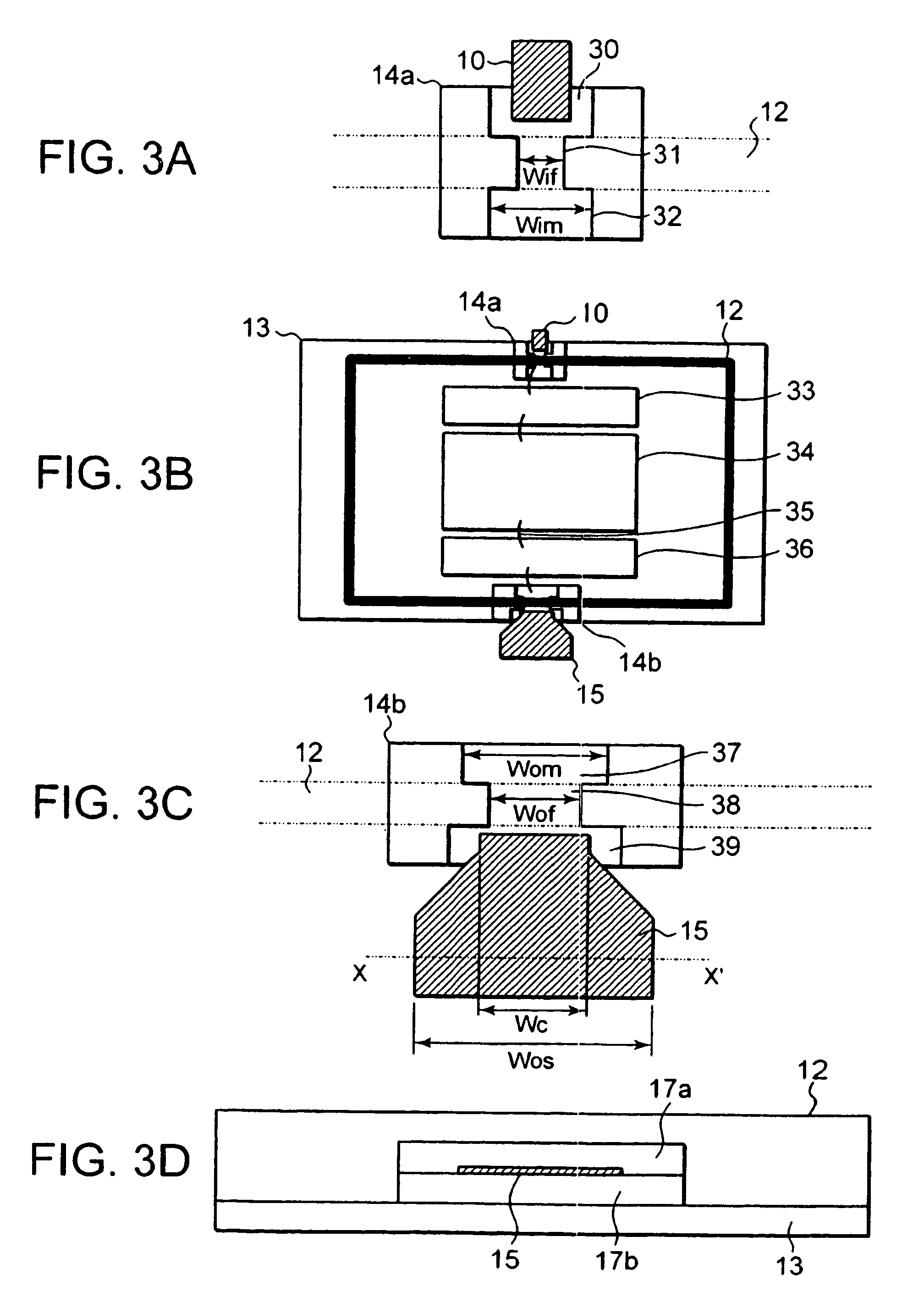
The present invention provides a high performance package for high frequency waves that can secure a sufficient current capacity at the output section and show good frequency characteristics. The package includes an hermetic box-shaped high frequency package containing a high frequency electronic circuit in the inside and shielded by a conductor. The input terminal and the output terminal are partly led out to the outside of the high frequency package. The package also includes an input side feed-through section and an output side feed-through section. The input side feed-through section has a predetermined characteristic impedance, while the output side feed-through section has a lower characteristic impedance as viewed from the output terminal side. This allows for a larger electric current capacity at the output section and good frequency characteristics. The package is designed to secure a sufficient current capacity at the output section and show good frequency characteristics.

Problems solved by technology

Then, a large ohm loss is produced when an electric current is flowed to a line showing such a relatively high resistance.
For this reason, there arises a problem that the applied voltage is not effectively conveyed to a semiconductor chip and the line can be fused by Joule heat generated when an electric current flows through the resistance components at the output terminal side to make it impossible to obtain a sufficient current capacity.
However, such a package also has high resistance components at the output side to make it impossible to obtain a sufficient current capacity and hence can give rise to the above described problem.
Additionally, such a package is also accompanied by a drawback that the high frequency characteristics are damaged when the line width of the input terminal or the output terminal is changed abruptly.

Method used


Image

  • Package for high frequency waves containing high frequency electronic circuit
  • Package for high frequency waves containing high frequency electronic circuit
  • Package for high frequency waves containing high frequency electronic circuit

Examples


Embodiment Construction

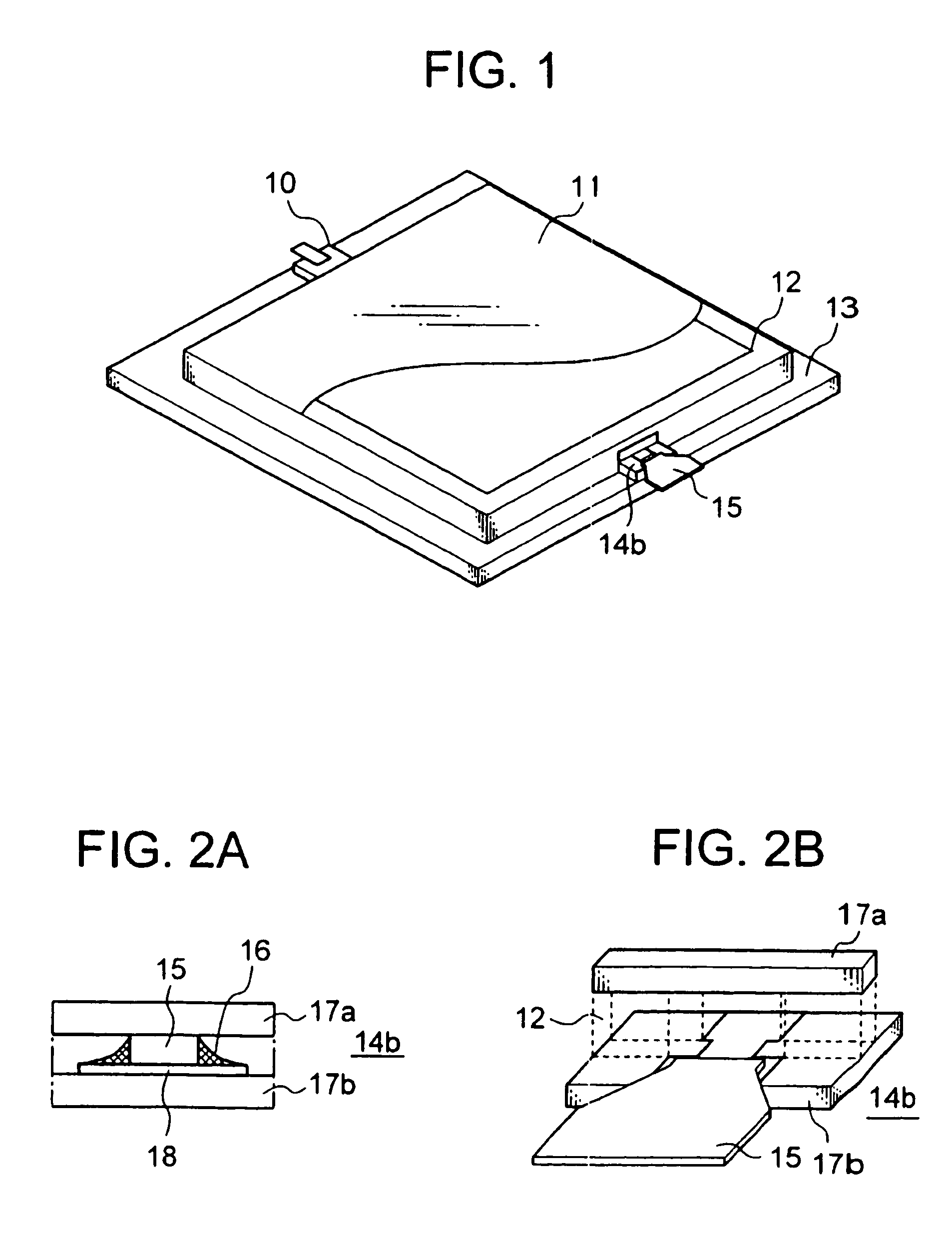
[0015]Now, the present invention will be described in greater detail by referring to the accompanying drawings that illustrate a preferred embodiment of the invention.

[0016]FIG. 1 is a schematic bird's-eye view of an embodiment of package for high frequency waves according to the present invention. The lower grounded metal plate 13 of the embodiment of package for high frequency waves needs to be made of a metal showing good grounded characteristics and, at the same time, a good thermal conductivity. Examples of metals that can be used for the grounded metal plate include Cu, CuW (copper tungsten) and CuMo (copper molybdenum). A ceramic plate having a thickness of about 0.6 mm is used as terminal forming substrate, which will make a lower dielectric 17b as will be described hereinafter.

[0017]A metal frame 12 that is typically about 0.7 mm width and about 5 to 8 mm high and made of Cu or an alloy of Fe, Ni and Co is bonded onto the surface of the grounded metal plate 13.

[0018]The met...


PUM


Abstract

In an embodiment of the invention, a package for high frequency waves mounted by a high frequency electronic circuit comprises an hermetic box-shaped high frequency package containing a high frequency electronic circuit in the inside and shielded by a conductor, an input terminal and an output terminal partly led out to the outside of the high frequency package, an input side feed-through section having one of its opposite ends connected to the input terminal and the other end connected to the high frequency electronic circuit and having a predetermined characteristic impedance; and an output side feed-through section having one of its opposite ends connected to the output terminal and the other end connected to the high frequency electronic circuit and having a characteristic impedance lower than the characteristic impedance of the input side feed-through section as viewed from the output terminal side.

Description

CROSS-REFERENCE TO RELATED APPLICATION[0001]This invention contains subject matter related to Japanese Patent Application JP 2005-266938 filed on Sep. 14, 2005, the entire contents of which are incorporated herein by reference.BACKGROUND OF THE INVENTION[0002](1) Field the Related Art[0003]The present invention relates to a package for high frequency waves and, more particularly, it relates to a high performance package for high frequency waves that enables outputting a large electric current.[0004](2) Description of the Related Art[0005]Devices and instruments are generally designed as 50Ω type in the field of microwaves.[0006]Similarly, as for packages for high frequency waves that contain elements for high frequency waves and matching circuits, characteristic impedances are generally designed as 50Ω type as viewed from the input terminal and the output terminal. Additionally, the input terminal and the output terminal are normally made to show a same profile and a same size regar...

Claims


Application Information

Patent Timeline
Patent Type & Authority Patents(United States)
IPC IPC(8): H03H7/38
CPCH01L23/552H01P5/02H01L23/66H01L2924/1305H01L2223/6627H01L2224/49175H01L2924/01025H01L2924/14H01L2924/1423H01L2924/1903H01L2924/30107H01L2924/3011H01L2924/3025H01L24/49H01L2924/00H01L2924/30111H01L2924/00014H01L2224/45014H01L2224/45099H01L2224/45015H01L2924/207H01L2924/206H01L23/48
Inventor TAKAGI, KAZUTAKA
Owner KK TOSHIBA
Learn More