
Operating method of non-volatile memory device

a non-volatile memory and operating method technology, applied in semiconductor devices, digital storage, instruments, etc., can solve the problems of high power consumption of the device, the inability to minimize the device, and the speed of performing the operation needs to be improved, so as to achieve the effect of very fast operation speed

Active Publication Date: 2008-12-09
MACRONIX INT CO LTD
View PDF61 Cites 42 Cited by
  • Summary
  • Abstract
  • Description
  • Claims
  • Application Information

AI Technical Summary

Benefits of technology

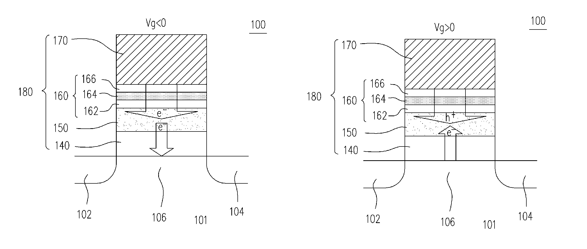
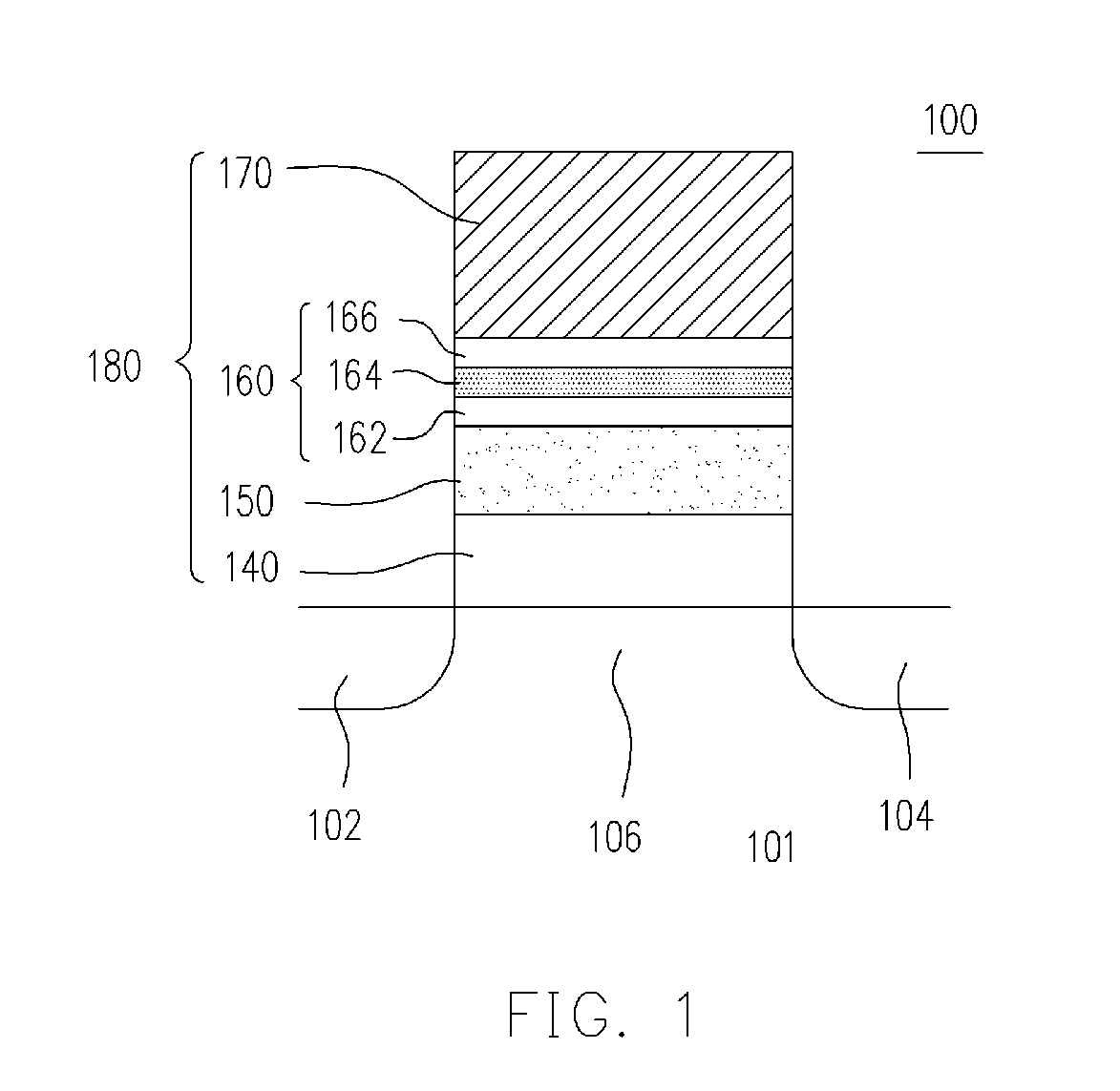
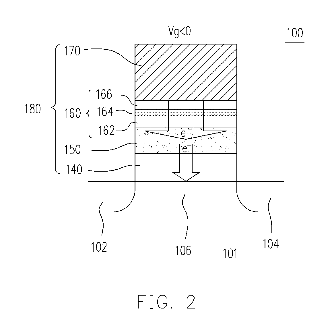
The present invention provides an operating method for a memory device that is not affected by the bird beak effect caused by shallow trench isolation structure and has a fast operation speed. The method includes a negative bias operation and a positive bias operation to inject electrons or holes into the charge storage layer of the memory cell through the multi-layer tunneling dielectric structure, resulting in the increasing or decreasing of the threshold voltage of the memory cell. The method also includes a first operation of programming or erasing the memory cell. The reliability of the memory device is not affected by the negative bias, and the operation speed is not affected by the positive bias. The materials used for the various layers in the memory device are also provided.

Problems solved by technology

In a present NVM, the tunneling oxidation layer is disposed on the channel so that the bird beak effect caused by shallow trench isolation structure affects the tunneling oxidation layer severely, thus, the device cannot be minimized.
On the other hand, high voltage is required by the electron tunneling programming or erasing operation of the present NVM, thus, the power consumption of the device is high, and the speed of performing the operations needs to be improved.

Method used


Image

  • Operating method of non-volatile memory device
  • Operating method of non-volatile memory device
  • Operating method of non-volatile memory device

Examples


Embodiment Construction

[0048]Herein the present invention and the exemplary embodiments thereof will be explained in detail with reference to the figures. It should be noted that the figures represent very simplified formats of the embodiments and are not drawn to accurate proportions. Wherever possible, like reference numerals refer to the like elements in all the figures. According to the present disclosure, the direction terms used in the figures, such as top, bottom, left, right, up, down, on, below, under, in front, and behind are used referring to the figures for the convenience of understanding. Such direction terms along with the descriptions to the figures should not be understood as limitations unmentioned in following claims to the scope of the present invention. It should be understood that even the present disclosure is explained with reference to some explanatory embodiments, such embodiments are not for limiting the scope of the present invention, and moreover, the processes and structures ...


PUM


Abstract

An operating method of non-volatile memory device is provided. The device includes memory cells having a semiconductor substrate, a stack layer, and source and drain regions disposed below a surface of the substrate and separated by a channel region. The stack layer includes an insulating layer disposed on the channel region, a charge storage layer disposed on the insulating layer, a multi-layer tunneling dielectric structure on the charge storage layer, and a gate disposed on the multi-layer tunneling dielectric structure. A negative bias is supplied to the gate to inject electrons into the charge storage layer through the multi-layer tunneling dielectric structure by −FN tunneling so that the threshold voltage of the device is increased. A positive bias is supplied to the gate to inject holes into the charge storage layer through the multi-layer tunneling dielectric structure by +FN tunneling so that the threshold voltage of the device is decreased.

Description

CROSS-REFERENCE TO RELATED APPLICATION[0001]This application claims the priority benefit of Taiwan application serial no. 95122001, filed Jun. 20, 2006. All disclosure of the Taiwan application is incorporated herein by reference.BACKGROUND OF THE INVENTION[0002]1. Field of the Invention[0003]The present invention relates to an operating method of a memory device. More particularly, the present invention relates to an operating method of a non-volatile memory device.[0004]2. Description of Related Art[0005]Non-volatile memory (NVM) is a semiconductor memory which can continue to store data after power is turned off. NVM includes mask read-only memory (Mask ROM), programmable read-only memory (PROM), erasable programmable read-only memory (EPROM), electrically erasable programmable read-only memory (EEPROM), and flash memory. NVM has been broadly applied in semiconductor industry and is a memory researched and developed for preventing program data loss. Generally, NVM can be programm...

Claims


Application Information

Patent Timeline
Patent Type & Authority Patents(United States)
IPC IPC(8): G11C11/34
CPCG11C16/0466G11C16/0483H01L21/28282H01L27/115H01L27/11568H01L29/42324H01L29/513H01L29/40117H10B69/00H10B43/30H01L29/66833
Inventor LUE, HANG-TINGLAI, ERH-KUNWANG, SZU-YU
Owner MACRONIX INT CO LTD
Learn More