Photoelectric conversion device and image pick-up system using the photoelectric conversion device
a technology of photoelectric conversion device and conversion device, which is applied in the direction of radio frequency control device, television system, television system scanning details, etc., and can solve problems such as lowering efficiency
- Summary
- Abstract
- Description
- Claims
- Application Information
AI Technical Summary
Benefits of technology
Problems solved by technology
Method used
Image

Examples
first embodiment
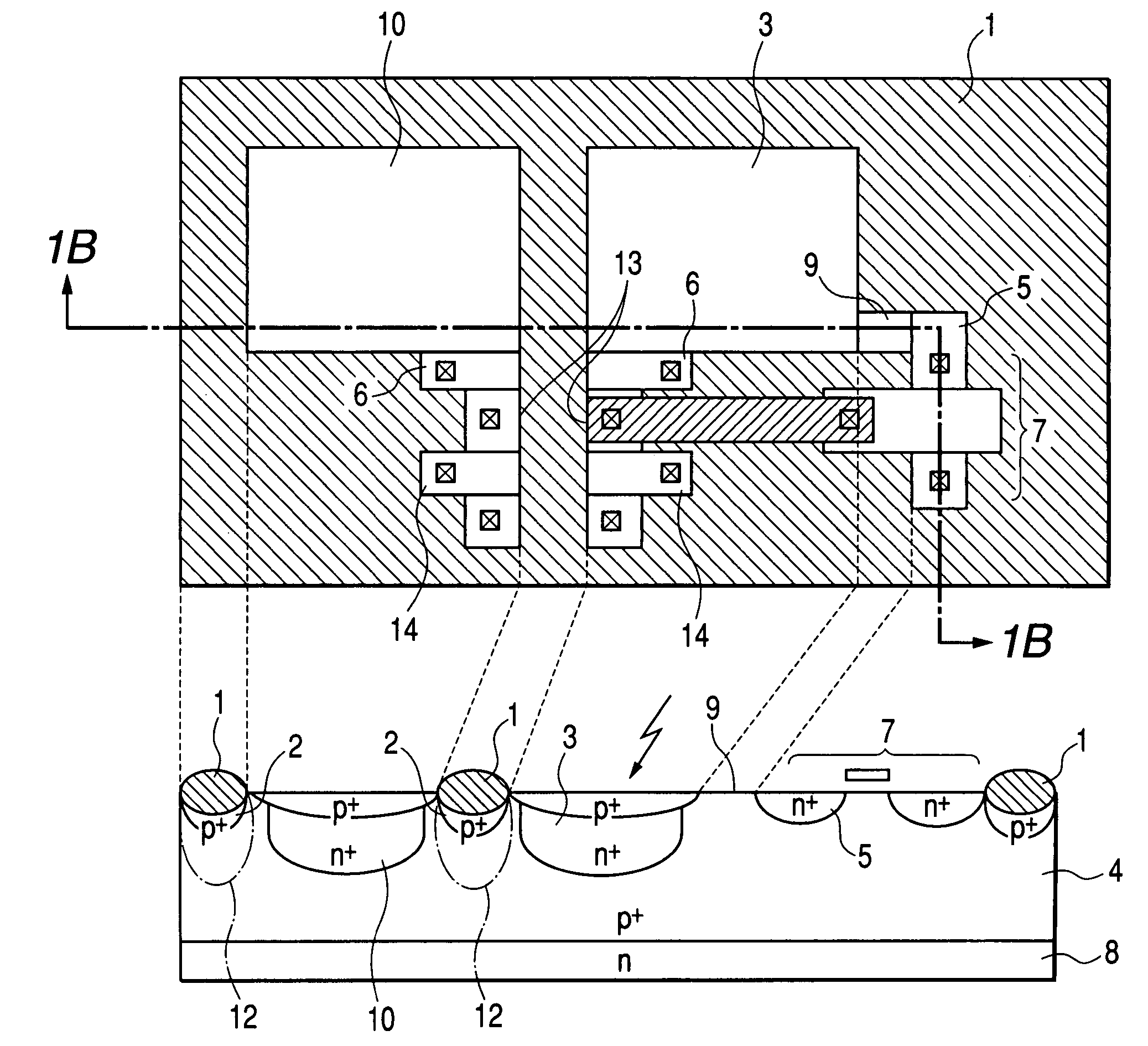
[0032]FIG. 1A is a plan view showing the structure of a photoelectric conversion device according to a first embodiment of the present invention, and FIG. 1B is a schematic sectional view taken along the line 1B-1B of FIG. 1A. As shown in FIGS. 1A and 1B, a photodiode (to serve as a photoelectric conversion region) 3 is formed in a p-well 4. Electric charges accumulated in the photodiode 3 are sent to a floating diffusion region 13 and to a gate of a MOS transistor 7, which is connected to the floating diffusion region 13, when the electric potential of a transfer electrode 6 is set to the high level. The MOS transistor 7 amplifies the electric charges to output signals. As shown in FIG. 1B, the photodiode 3 adjoins to a photodiode 10 (to serve as a photoelectric conversion region) of an adjacent pixel with a selectively oxidized film 1 separating the photodiode 3 from the photodiode 10 (the selectively oxidized film 1 surrounds the perimeters of the photodiodes 3 and 10). Reference...
second embodiment
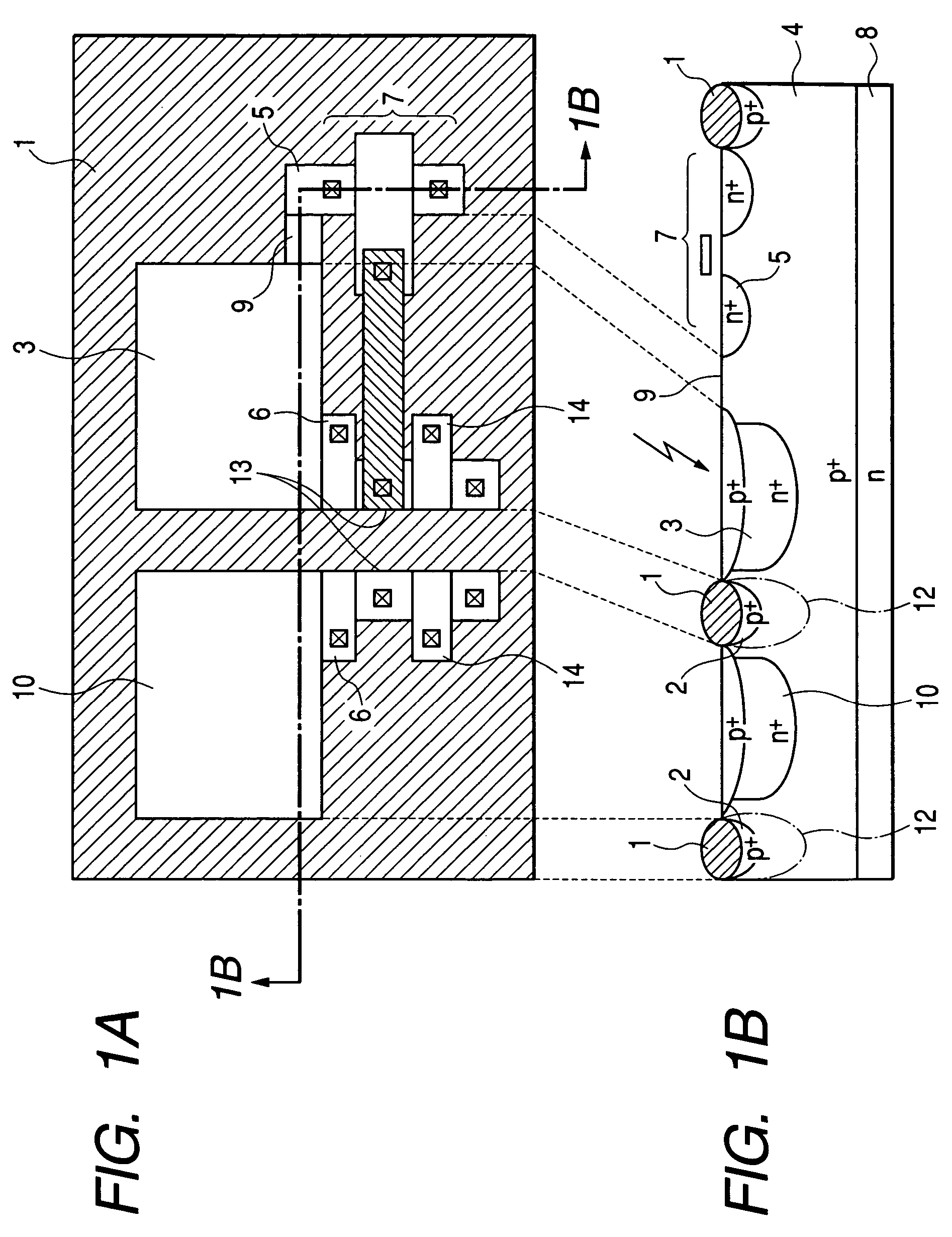
[0035]FIG. 2A is a plan view showing the structure of a photoelectric conversion device according to a second embodiment of the present invention, and FIG. 2B is a schematic sectional view taken along the line 2B-2B of FIG. 2A. In FIGS. 2A and 2B, structural members that are identical with those in FIGS. 1A and 1B are denoted by the same reference numerals, and explanations thereof are omitted.
[0036]This embodiment differs from the first embodiment in that a buried potential barrier layer (to serve as a buried isolation region) 11 is formed under the channel stopping layer 2 using a p type impurity to surround the photodiodes 3 and 10. A nick region 29 serves as an overflow channel region similar to the-overflow channel region 9 of the first embodiment. Specifically, the nick region 29 is a region where the selectively oxidized film 1 and the channel stopping layer 2 are not formed. FIG. 2B mainly deals with impurity distribution. As to potential distribution, potentials are distrib...
third embodiment
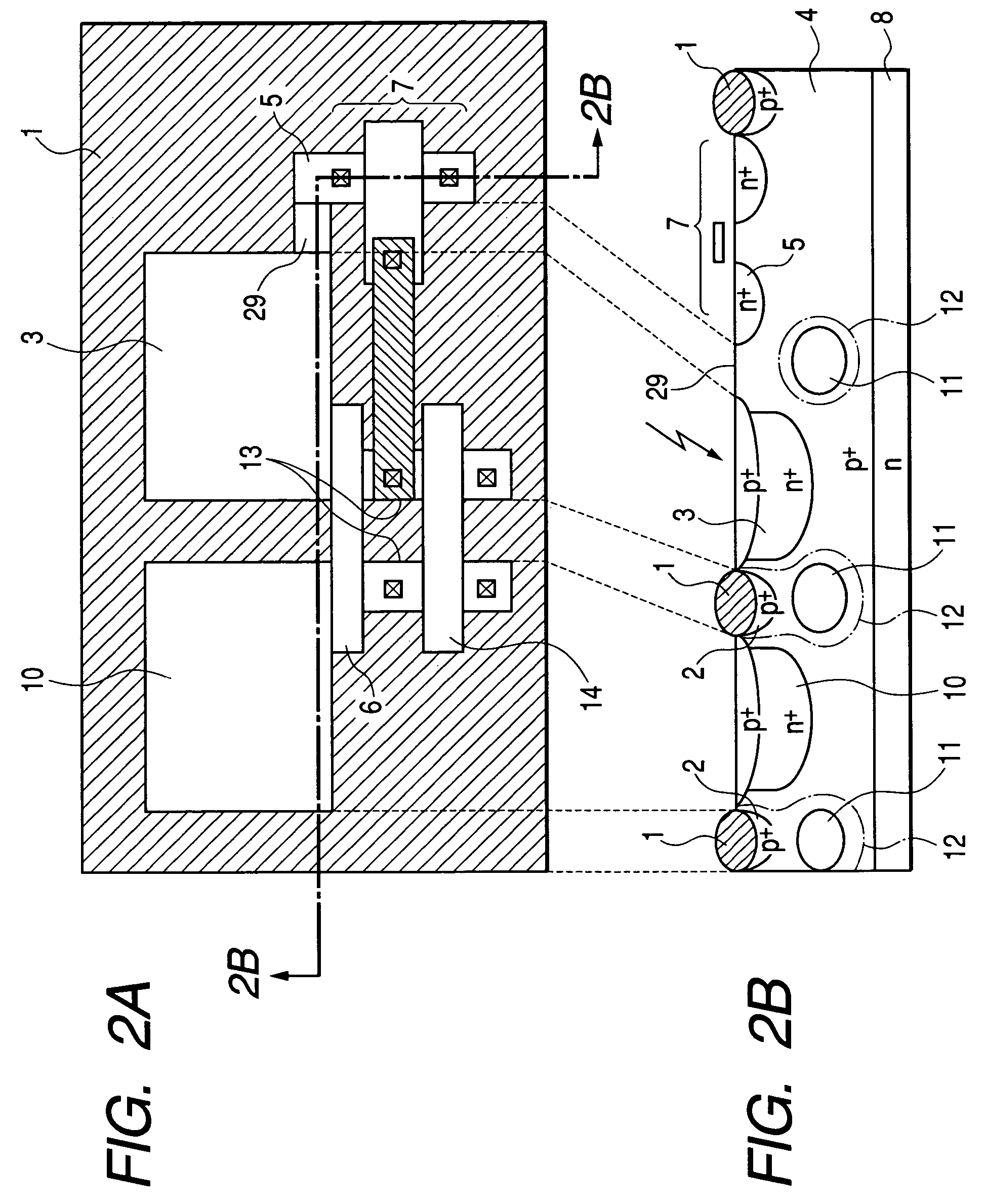
[0038]FIG. 3A is a plan view showing the structure of a photoelectric conversion device according to a third embodiment of the present invention, and FIG. 3B is a schematic sectional view taken along the line 3B-3B of FIG. 3A. In FIGS. 3A and 3B, structural members that are identical with those in FIGS. 2A and 2B are denoted by the same reference numerals, and explanations thereof are omitted.
[0039]In this embodiment, the buried potential barrier layer 11 and the channel stopping layer 2 above the layer 11 surround the photodiodes 3 and 10 as in the second embodiment. The difference between the two embodiments is that, in the third embodiment, the potential barrier layer 11 is absent only in a nick region 39, which is between the photodiode 3 and the drain region 5.
[0040]In FIG. 3B, potentials are distributed in the region (potential barrier) 12 that is a bit larger than the channel stopping layer 2 and the potential barrier layer 11. The region 12 is indicated by a dot-dash line in...
PUM
 Abstract
Description
Claims
Application Information
 - R&D
- Intellectual Property
- Life Sciences
- Materials
- Tech Scout
- Unparalleled Data Quality
- Higher Quality Content
- 60% Fewer Hallucinations
Browse by: Latest US Patents, China's latest patents, Technical Efficacy Thesaurus, Application Domain, Technology Topic, Popular Technical Reports.
© 2025 PatSnap. All rights reserved.Legal|Privacy policy|Modern Slavery Act Transparency Statement|Sitemap|About US| Contact US: help@patsnap.com