
Apparatus, system, and method for modifying memory voltage and performance based on a measure of memory device stress

a memory device and stress measurement technology, applied in pulse generators, pulse techniques, instruments, etc., can solve the problems of increasing potential performance, operating the memory device at a higher voltage may have one or more adverse consequences, and the voltage of the memory device is decreased, so as to reduce increase the stress of the memory device, and slow the timing of the memory device

Inactive Publication Date: 2008-10-28
LENOVO GLOBAL TECH INT LTD
View PDF5 Cites 19 Cited by
  • Summary
  • Abstract
  • Description
  • Claims
  • Application Information

AI Technical Summary

Benefits of technology

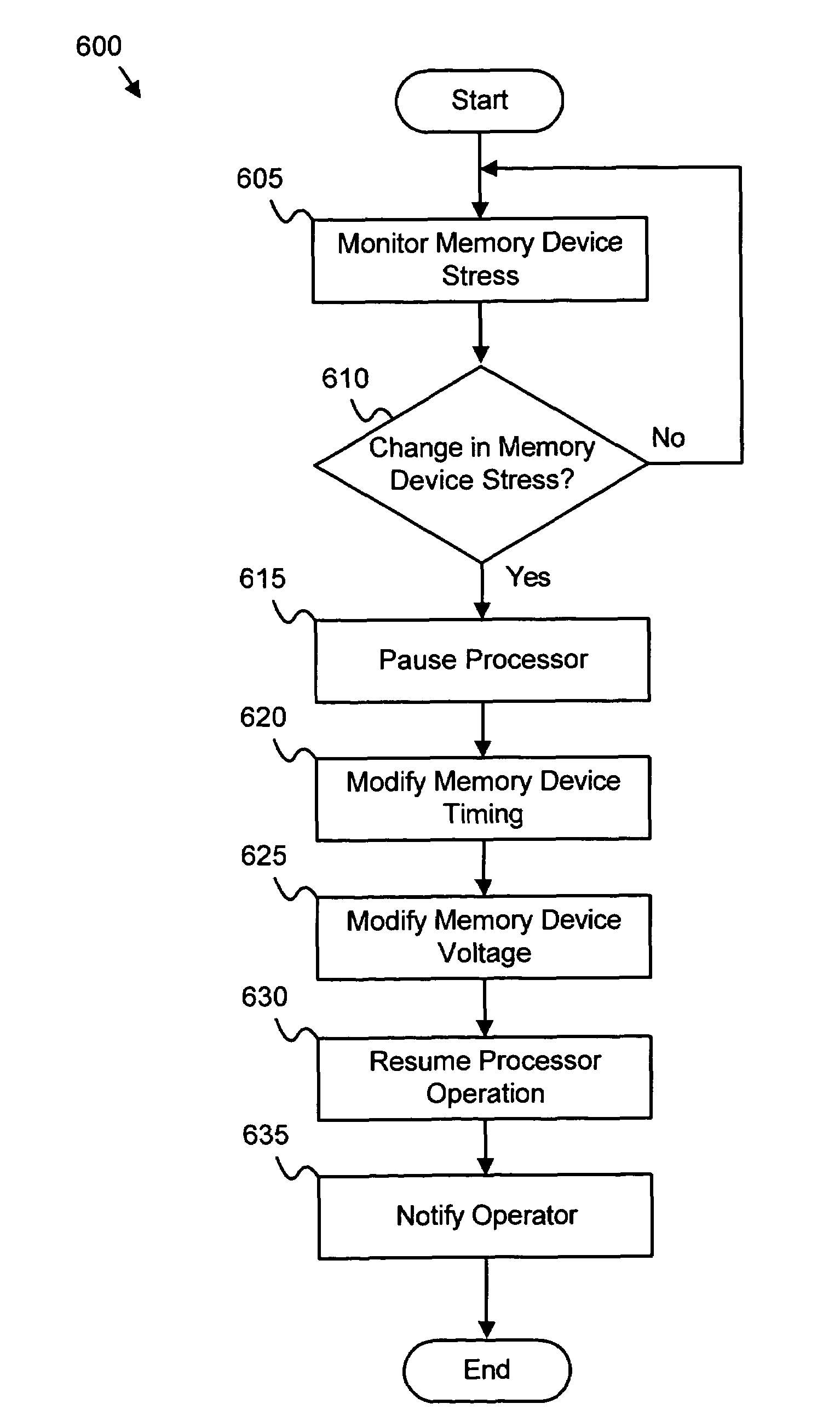
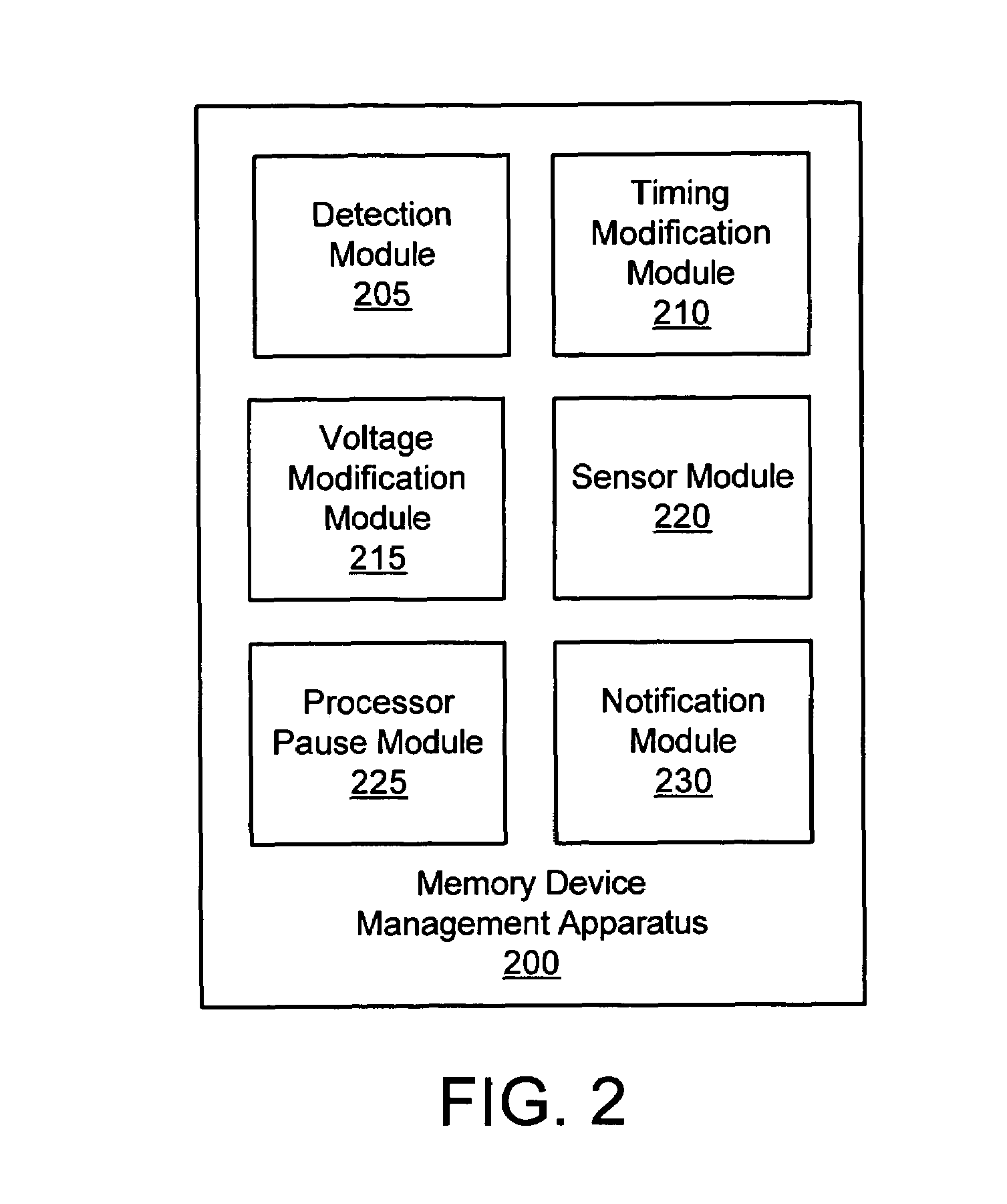
[0013]The timing modification module modifies memory device timing in response to the change of the memory device stress. For example, if the detection module detects increased memory device stress as indicated by an increase in memory device data error rate, the timing modification module may slow the timing of the memory device. In an alternate example, if the detection module detects decreased memory device stress as indicated by a decrease in temperature, the timing modification module may speed the timing of the memory device.
[0015]In one embodiment, the processor pause module pauses the operation of a processor module while the timing modification module modifies the memory device timing and the voltage modification module modifies the memory device voltage. For example, if the detection module detects decreased memory device stress, the processor pause module may pause the operation of the processor module. The timing modification module may subsequently speed the memory device timing and the voltage modification module may increase the memory device voltage. The processor pause module may then allow the processor module to resume operation. The apparatus modifies the memory device voltage and timing in response to changes in the memory device stress, supporting increased memory device performance while mitigating the adverse consequences of increased performance.
[0018]The detection module detects a change of memory device stress. The timing modification module modifies memory device timing in response to the change of the memory device stress. The voltage modification module modifies memory device voltage in response to the change of the memory device stress by directing the voltage regulator module to change the memory device voltage. In one embodiment, the system further includes a notification module. The notification module may notify an operator that the memory device requires replacement in response to an increase in the memory device stress. The system modifies memory device timing and voltage to mitigate increases in memory device stress and support increased memory device performance.
[0023]The present invention modifies the timing and the voltage of a memory device in response to a change in memory device stress. In addition, the present invention supports increased memory device performance while mitigating the adverse consequences of increased performance. These features and advantages of the present invention will become more fully apparent from the following description and appended claims, or may be learned by the practice of the invention as set forth hereinafter.

Problems solved by technology

Thus increasing memory device voltage increases potential performance while decreasing the memory device voltage decreases potential performance.
Unfortunately, operating the memory device at a higher voltage may have one or more adverse consequences.
As a result, the DPD may require more expensive cooling devices to maintain the desired temperature for the DPD.
Increasing the voltage and timing for the memory device may also increase the stress on elements of the memory device, increasing the risk of failure.
For example, one or more semiconductor gates comprising the memory device may be significantly more likely to fail at a higher voltage and temperature than at a lower voltage and temperature.

Method used


Image

  • Apparatus, system, and method for modifying memory voltage and performance based on a measure of memory device stress
  • Apparatus, system, and method for modifying memory voltage and performance based on a measure of memory device stress
  • Apparatus, system, and method for modifying memory voltage and performance based on a measure of memory device stress

Examples


Embodiment Construction

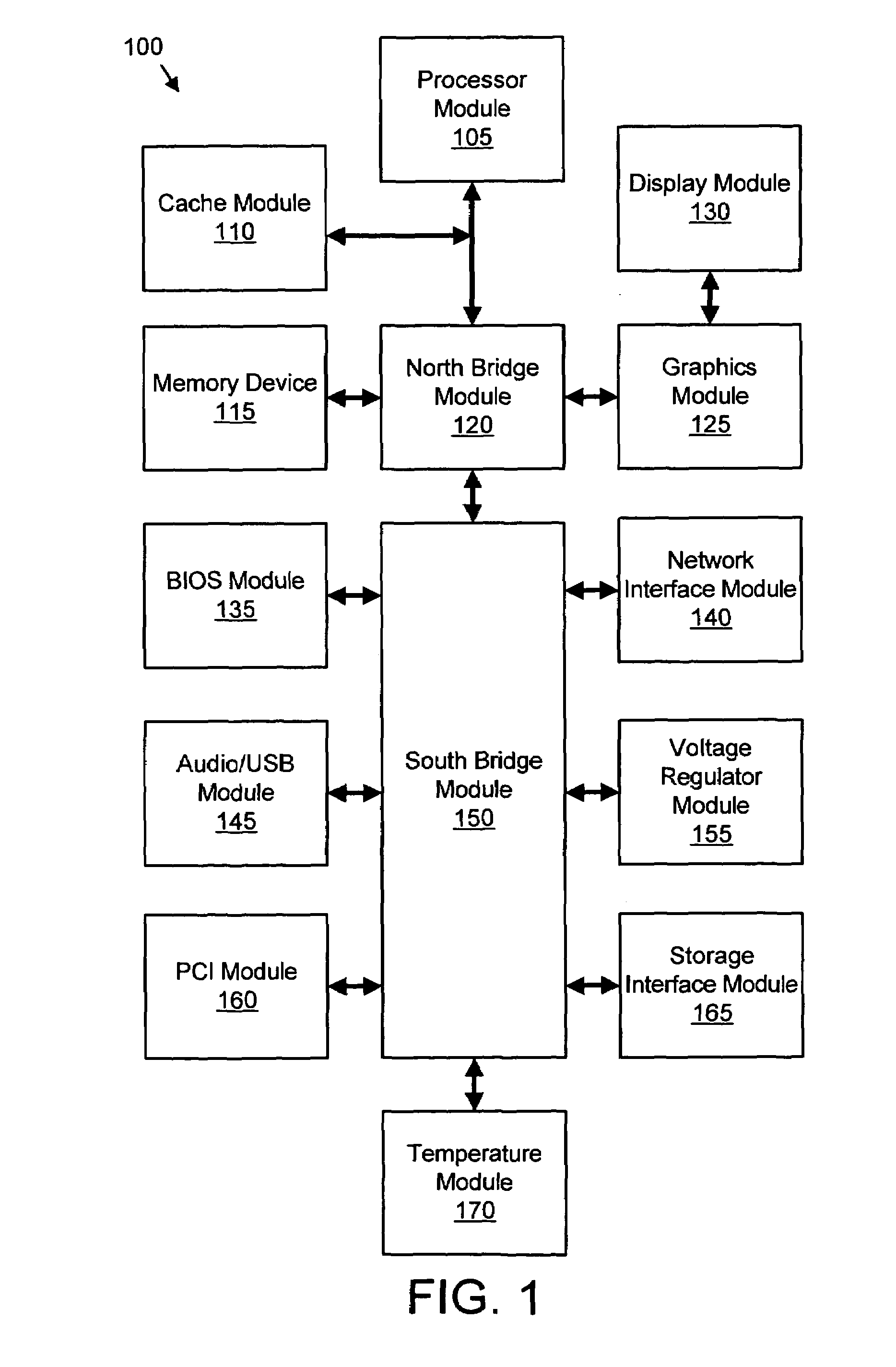
[0031]Many of the functional units described in this specification have been labeled as modules, in order to more particularly emphasize their implementation independence. For example, a module may be implemented as a hardware circuit comprising custom very large scale integration (“VLSI”) circuits or gate arrays, off-the-shelf semiconductors such as logic chips, transistors, or other discrete components. A module may also be implemented in programmable hardware devices such as field programmable gate arrays, programmable array logic, programmable logic devices or the like.

[0032]Modules may also be implemented in software for execution by various types of processors. An identified module of executable code may, for instance, comprise one or more physical or logical blocks of computer instructions, which may, for instance, be organized as an object, procedure, or function. Nevertheless, the executables of an identified module need not be physically located together, but may comprise ...


PUM


Abstract

An apparatus, system, and method are disclosed for modifying memory device timing and voltage. A detection module detects a change of memory device stress. A timing modification module modifies the memory device timing in response to the change of the memory device stress. In addition, a voltage modification module modifies the memory device voltage in response to the change of the memory device stress. In one embodiment, a processor pause module pauses the operation of a processor module while the timing modification module modifies the memory device timing and the voltage modification module modifies the memory device voltage.

Description

BACKGROUND OF THE INVENTION[0001]1. Field of the Invention[0002]This invention relates to modifying memory device voltage and more particularly relates to modifying memory device voltage and performance in response to changes in memory device stress.[0003]2. Description of the Related Art[0004]A data processing device (“DPD”) such as a server, computer workstation, router, mainframe computer, and the like typically uses a memory device such as dynamic random access memory (“DRAM”), static random access memory (“SRAM”), and the like to store instructions and data. For example, a processor module of the DPD may read and execute instructions from the memory device and read and process data from the memory device.[0005]The performance of the memory device directly affects the performance of the DPD. For example, a memory device with fast timing is able to deliver more instructions and data to the processor module during a specified time interval than a memory device with slow timing. As...

Claims


Application Information

Patent Timeline
Patent Type & Authority Patents(United States)
IPC IPC(8): G06F12/00G06F11/00G06F13/00G06F13/28G11C11/34G11C29/00G11C7/04H01L35/00H01L37/00H03K17/78H03K3/42
CPCG06F13/4072
Inventor CASES, MOISESDE ARAUJO, DANIEL N.PHAM, NAM HUUROUMBAKIS, MENAS
Owner LENOVO GLOBAL TECH INT LTD
Learn More