Optimization of critical dimensions and pitch of patterned features in and above a substrate

a technology of critical dimensions and pitch, applied in the direction of semiconductor devices, semiconductor/solid-state device details, electrical devices, etc., can solve the problems of increasing lithography costs and increasing the overall device cos

Active Publication Date: 2008-09-09
SANDISK TECH LLC
View PDF13 Cites 49 Cited by
  • Summary
  • Abstract
  • Description
  • Claims
  • Application Information

AI Technical Summary

Problems solved by technology

Pitch (the center-to-center distance between features of an integrated circuit) generally has been relaxed in higher layers due to the difficulty of accurately patterning and etching features over a surface which is not perfectly planar.
Smaller pitch increases lithography costs, however, increasing overall device cost.

Method used


Image

  • Optimization of critical dimensions and pitch of patterned features in and above a substrate
  • Optimization of critical dimensions and pitch of patterned features in and above a substrate
  • Optimization of critical dimensions and pitch of patterned features in and above a substrate

Examples


Embodiment Construction

[0027]Typically semiconductor devices are formed in a substrate, normally the surface of a semiconductor wafer, most often monocrystalline silicon. There has been steady pressure to decrease cost of semiconductor devices by decreasing pitch of patterned features in the substrate, allowing more devices to be packed into a given substrate area. It is common to form transistors, for example CMOS transistors, in the substrate while forming multiple wiring levels above the substrate.

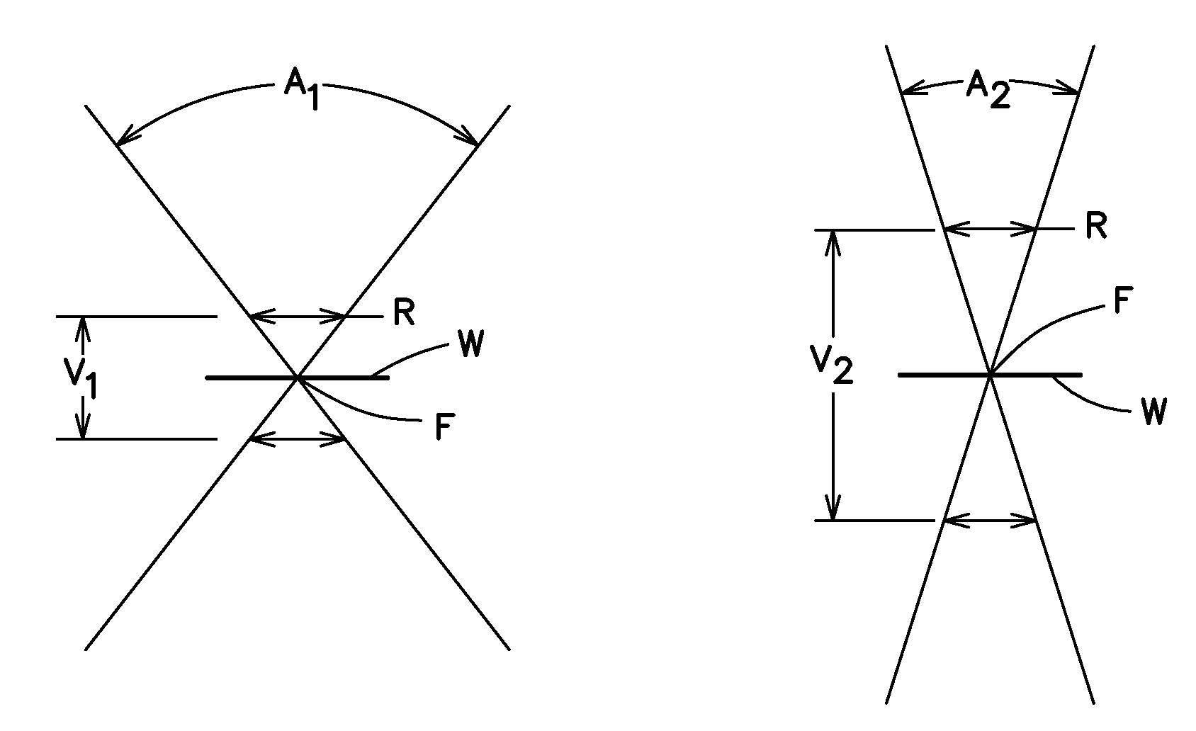
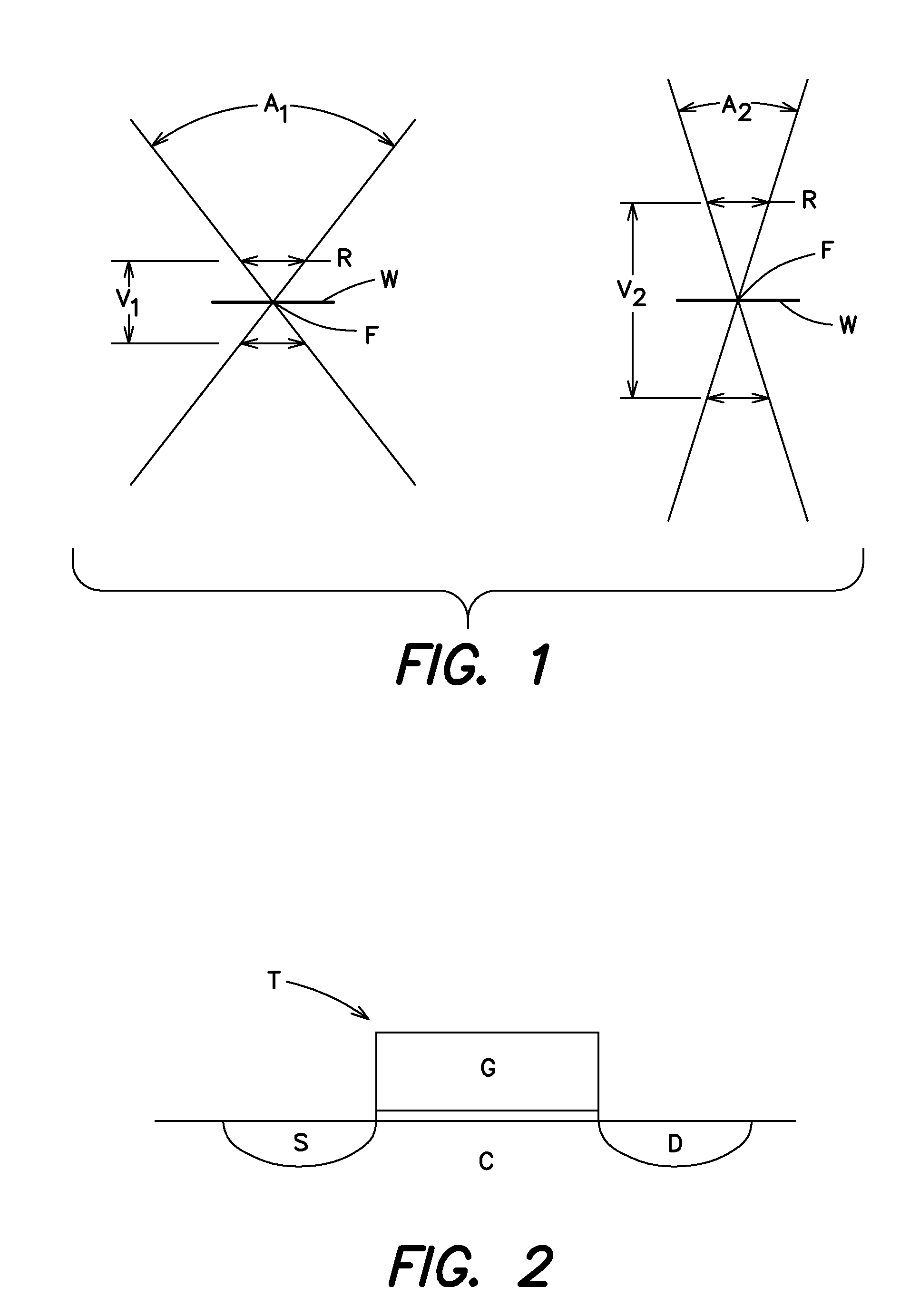
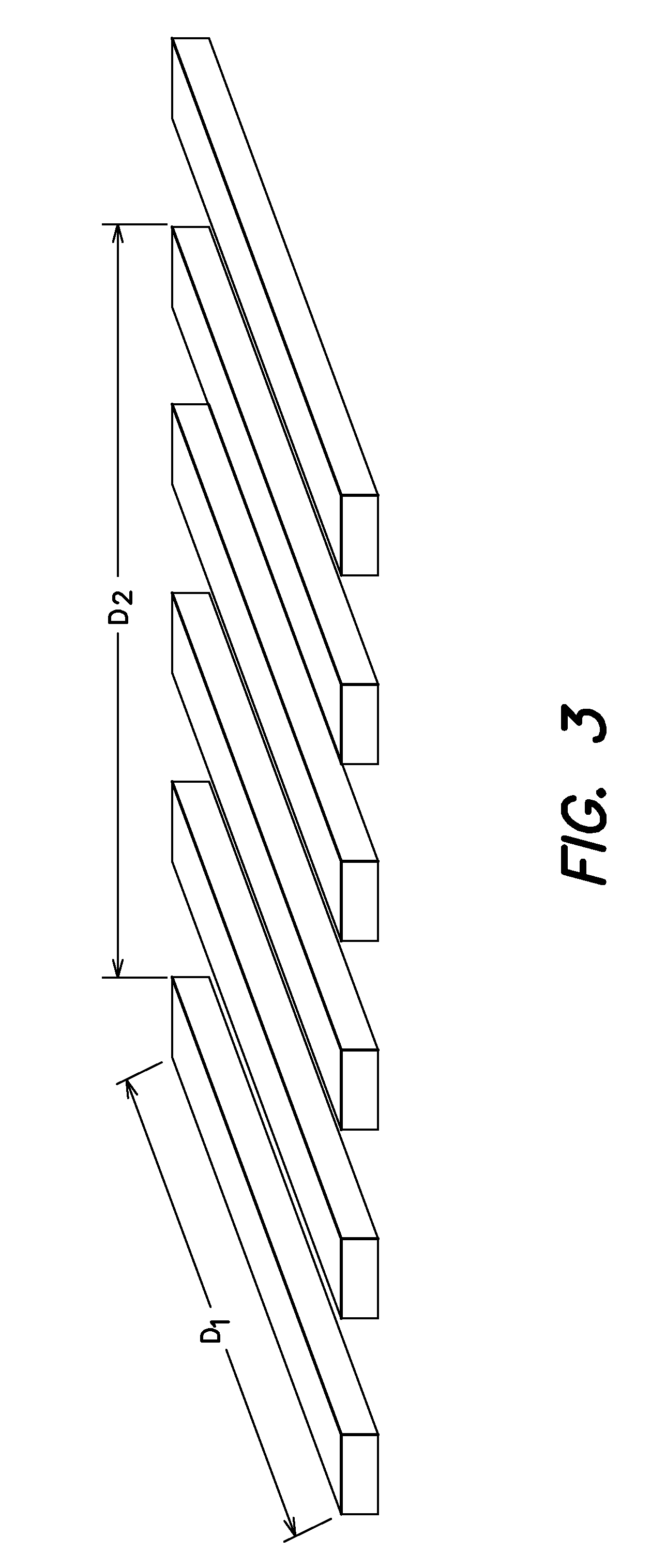
[0028]Device dimensions can be described by the terms pitch and critical dimension. Pitch was defined earlier as the center-to-center distance between features of an integrated circuit. This distance is apparent when features are regular or repeating; for example, when there is a plurality of parallel lines with consistent size and spacing. Pitch can be used to describe features without this regularity as well, however. When features are not regular or repeating, pitch is considered herein to be the sum of th...


PUM


Abstract

A die is formed with different and optimized critical dimensions in different device levels and areas of those device levels using photolithography and etch techniques. One aspect of the invention provides for a memory array formed above a substrate, with driver circuitry formed in the substrate. A level of the memory array consists of, for example, parallel rails and a fan-out region. It is desirable to maximize density of the rails and minimize cost of lithography for the entire memory array. This can be achieved by forming the rails at a tighter pitch than the CMOS circuitry beneath it, allowing cheaper lithography tools to be used when forming the CMOS, and similarly by optimizing lithography and etch techniques for a device level to produce a tight pitch in the rails, and a more relaxed pitch in the less-critical fan-out region.

Description

RELATED APPLICATIONS[0001]This application is related to Scheuerlein et al., U.S. application Ser. No. 10 / 728,451, “High Density Contact to Relaxed Geometry Layers,” filed on even date herewith, which application is hereby incorporated by reference.BACKGROUND OF THE INVENTION[0002]In traditional circuit layout for a semiconductor die, features are arranged most densely in the substrate and at the same or lower density in subsequent wiring layers formed above the substrate. Pitch (the center-to-center distance between features of an integrated circuit) generally has been relaxed in higher layers due to the difficulty of accurately patterning and etching features over a surface which is not perfectly planar. Topography and deviations from planarity tend to increase in higher layers. Moreover, for simplicity of layout, it is usual to make shorter connections in lower wiring layers, and longer connections in higher wiring layers. As wiring is longer in higher layers, slowing device spee...

Claims


Application Information

Patent Timeline
Patent Type & Authority Patents(United States)
IPC IPC(8): H01L29/80H01L31/112H01L23/528H01L27/105
CPCH01L23/528H01L27/105H01L2924/0002H01L2924/00
Inventor CLEEVES, JAMES M.SCHEUERLEIN, ROY E.
Owner SANDISK TECH LLC
Why Eureka
Try Eureka