
Ultra wide band, differential input/output, high frequency amplifier in an integrated circuit

a high frequency amplifier and integrated circuit technology, applied in the field of high frequency amplifiers, can solve the problems of difficult to fabricate a wide band amplifier on a die for use as an integrated circuit, and more difficult to fabricate an ultra wide band amplifier on a die with a constant gain, so as to increase the frequency bandwidth of the amplifier

Active Publication Date: 2008-07-15
HARRIS CORP
View PDF4 Cites 6 Cited by
  • Summary
  • Abstract
  • Description
  • Claims
  • Application Information

AI Technical Summary

Problems solved by technology

It is difficult to fabricate a wide band amplifier on a die for use as an integrated circuit (IC).
It is even more difficult to fabricate an ultra wide band amplifier on a die having a constant gain across a frequency band that spans from direct current (dc) up to a frequency in excess of 20 GHz.

Method used


Image

  • Ultra wide band, differential input/output, high frequency amplifier in an integrated circuit
  • Ultra wide band, differential input/output, high frequency amplifier in an integrated circuit
  • Ultra wide band, differential input/output, high frequency amplifier in an integrated circuit

Examples


Embodiment Construction

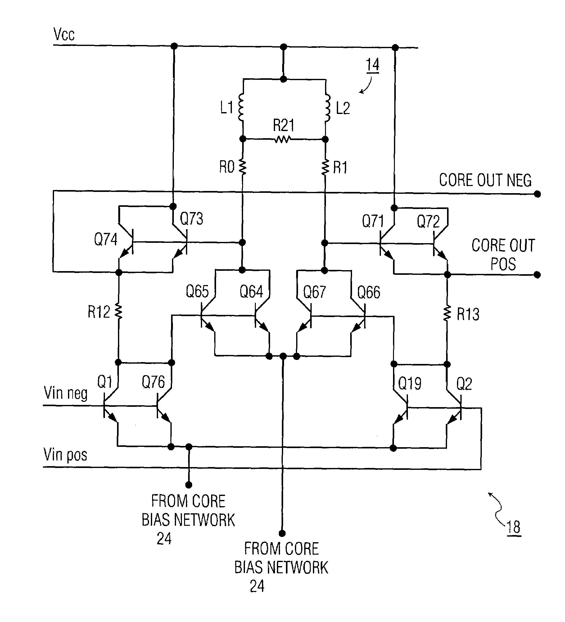
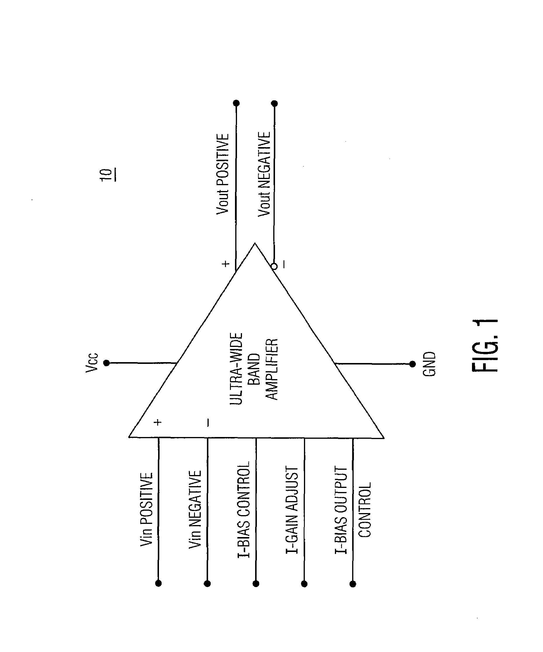
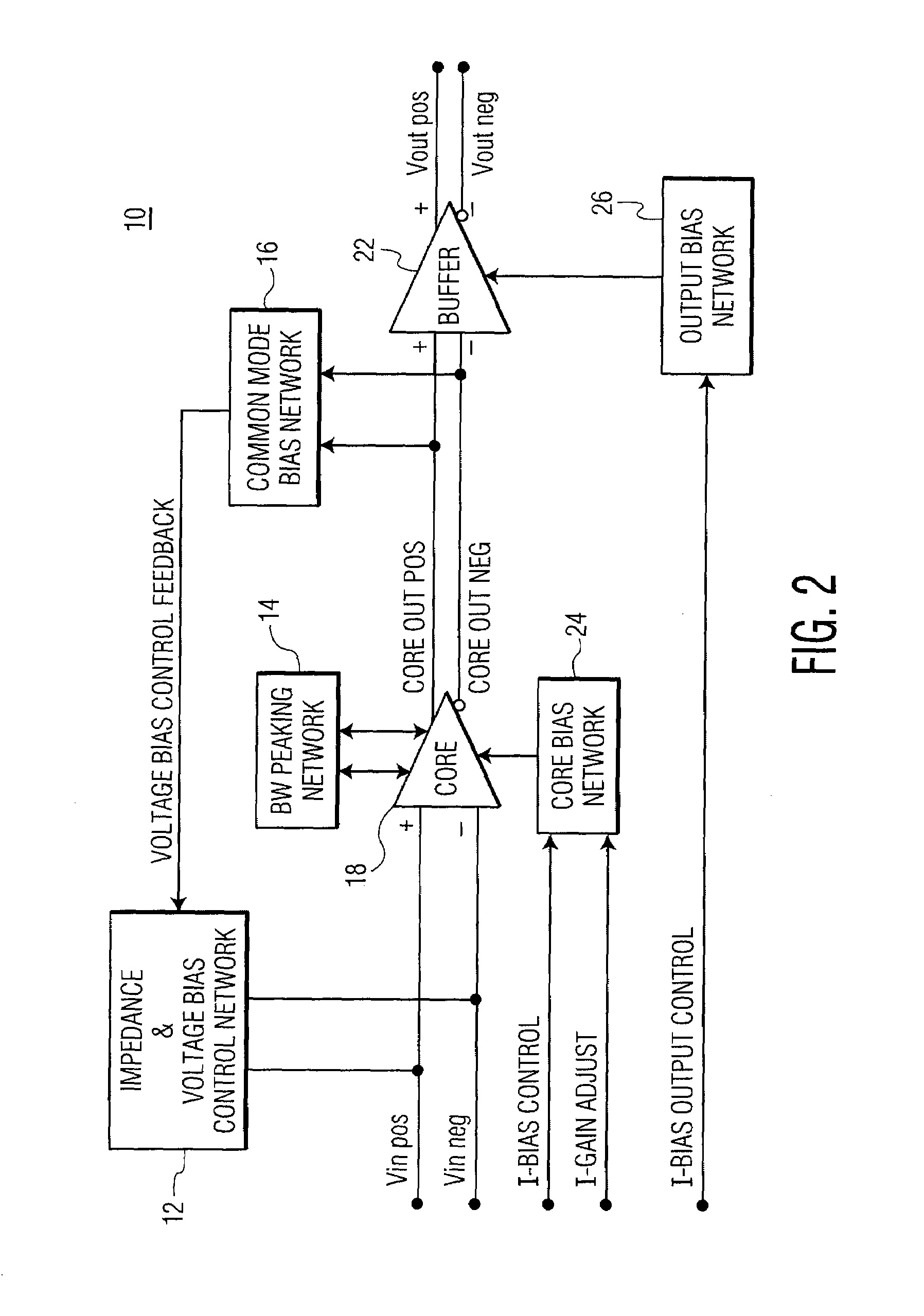
[0026]As will be described, the present invention provides an ultra wide band amplifier, operating between direct current (dc) and frequencies greater than 20 GHz. The present invention includes a bandwidth peaking network that extends the frequency response of the amplifier and provides a nearly constant gain across the ultra wide band of the amplifier. In addition, the present invention receives a pair of differential input signals and transmits a pair of differential output signals. The present invention also includes a controlled input impedance and a controlled output impedance. Moreover, the present invention operates with a low supply voltage and includes a common mode biasing method for AC applications, and an accurate fixed ratio bias tracking scheme. These features all contribute to advantageous improvements of an ultra wide band amplifier that is disposed on a die and fabricated for use in an integrated circuit (IC) or chip.

[0027]Referring to FIG. 1, there is shown a func...


PUM


Abstract

A wide band amplifier includes a core amplifier having input terminals and output terminals for, respectively, receiving differential input signals and providing amplified differential output signals. A bandwidth peaking network is coupled to the core amplifier and includes (a) a first coil and a first resistor connected in series and (b) a second coil and a second resistor connected in series. The first coil and resistor and the second coil and resistor, respectively, are coupled to the core amplifier for receiving the amplified differential output signals. The bandwidth peaking network is configured to increase the frequency bandwidth of the amplifier. The bandwidth peaking network includes (a) a first node formed between the first coil and resistor, (b) a second node formed between the second coil and resistor, and (c) a third resistor is connected between the first node and the second node. This resistor is free of current flow at low frequency operation of the amplifier.

Description

CROSS REFERENCE TO RELATED APPLICATIONS[0001]This application claims priority of U.S. Provisional Patent Application Ser. No. 60 / 817,387, filed Jun. 29, 2006.FIELD OF THE INVENTION[0002]The present invention relates, in general, to a high frequency amplifier. More specifically, the present invention relates to an ultra wide band (from dc to greater than 20 GHz), substantially constant gain amplifier that is fabricated as an integrated circuit, and has differential input / output signal capabilities.BACKGROUND OF THE INVENTION[0003]An amplifier that provides linear amplification, as compared to an amplifier that operates in the saturation region, receives an input signal and generates an output signal having a predetermined amount of gain. The frequency components of the output signal are generally similar to the frequency components of the input signal.[0004]In some applications, there is a requirement that an amplifier provide a constant gain across its entire frequency response or b...

Claims


Application Information

Patent Timeline
Patent Type & Authority Patents(United States)
IPC IPC(8): H03F3/18
CPCH03F1/42H03F3/45085H03F3/45475H03F3/45497H03F3/45941H03F3/195H03F2203/45696H03F2200/36H03F2203/45178H03F2203/45352H03F2203/45418H03F2203/45434H03F2203/45576H03F2203/45596H03F2203/45601H03F2203/45622H03F2203/45638
Inventor WYATT, MICHAEL A.
Owner HARRIS CORP
Learn More