
Method and apparatus for an improved power amplifier

a power amplifier and amplifier technology, applied in amplifiers, amplifiers with semiconductor devices/discharge tubes, electrical apparatus, etc., can solve the problems of low breakdown voltage, unwanted current flow across the device, and amplifiers, especially those used with wireless communication devices, and achieve high output power and power-added efficiency. high

Active Publication Date: 2008-04-15
QORVO INT PTE LTD
View PDF4 Cites 14 Cited by
  • Summary
  • Abstract
  • Description
  • Claims
  • Application Information

AI Technical Summary

Benefits of technology

The solution enables high output power and power-added efficiency while preventing breakdown and maintaining performance under load mismatch conditions, extending battery life and reducing energy wastage.

Problems solved by technology

Known power amplifiers, particularly those used with wireless communication devices, face a variety of challenges.
This desire magnifies potential problems, because among other things, CMOS circuitry typically has very low breakdown voltages.
Excess electrons or holes are generated by high electric fields, creating an unwanted flow of current across the device.
Eventually, permanent damage will occur.
Whenever a forward voltage is placed on the gate, there is a potential for breakdown across the oxide, in which the gate can short to the source, drain or bulk regions of the MOSFET.
Even if no breakdown occurs across the gate, a long-term threshold voltage shift can occur, which causes the characteristics of the MOSFET to shift, if the gate source voltage is kept too high for a long period of time.
In another challenge, known power amplifiers are usually designed with single-ended power amplifiers driving simple, off-chip, high-Q (low-loss) matching circuits.
Under poor load match conditions, excessive energy can be reflected back to the output stage of the power amplifier.
This condition will cause a shift in the output match, resulting in lower RF output power and greatly reduced efficiency.
More problematic is the fact that such miss-match conditions generally result in much higher signal swings across the devices, leading to voltage breakdown.
Breakdown conditions generally result in permanent damage to the power amplifier.
Reflections from the load cause similar problems for these topologies, as mentioned above.
In yet another challenge to known amplifiers, when a transistor breaks down, excessive current flows and localized, permanent damage occurs.
After the breakdown event, most devices are no longer usable.
In some cases, such breakdown is not catastrophic, but does degrade device performance.
Unfortunately, this approach leads to reduced power output and lower efficiency.
In IC processes such as low-voltage CMOS, there is little headroom to begin with, so the back-off approach carries a heavy penalty.
In general, high-breakdown devices tend to be built in specialized semiconductor processes, usually at higher costs than other IC processes.
Clamps limit the voltage by shunting current from the output devices, thus limiting voltage swing to save levels.
However, this shunted current is essentially wasted, resulting in lower efficiency.
In a still further challenge, the requirements for high density, high speed CMOS logic are generally at odds with the requirements for RF power amplifiers.
However, operation at high signal swings, such as those needed for power amplifiers, is very difficult.
In general, such higher voltage semiconductor processes are more expensive than standard “vanilla” CMOS.
Additionally, the need to go off-chip with the RF signal results in lower efficiency.
In yet another challenge, known devices fail to provide both high gain and high efficiency.
This low gain hinders this type of amplifier.
Other known amplifier designs may have better gain, but are power limited.

Method used


Image

  • Method and apparatus for an improved power amplifier
  • Method and apparatus for an improved power amplifier
  • Method and apparatus for an improved power amplifier

Examples


Embodiment Construction

[0076]It is to be understood that both the foregoing general description and the following detailed description are exemplary and explanatory only and are not restrictive of the invention, as claimed. It may be noted that, as used in the specification and the appended claims, the singular forms “a,”“an,” and “the” include plural referents unless the context clearly dictates otherwise. Thus, for example, reference to “a material” may include mixtures of materials, reference to “a resistor” may include multiple resistors, and the like. References cited herein are hereby incorporated by reference in their entirety, except to the extent that they conflict with teachings explicitly set forth in this specification.

[0077]In this specification and in the claims which follow, reference will be made to a number of terms which shall be defined to have the following meanings:

[0078]“Optional” or “optionally” means that the subsequently described circumstance may or may not occur, so that the des...


PUM


Abstract

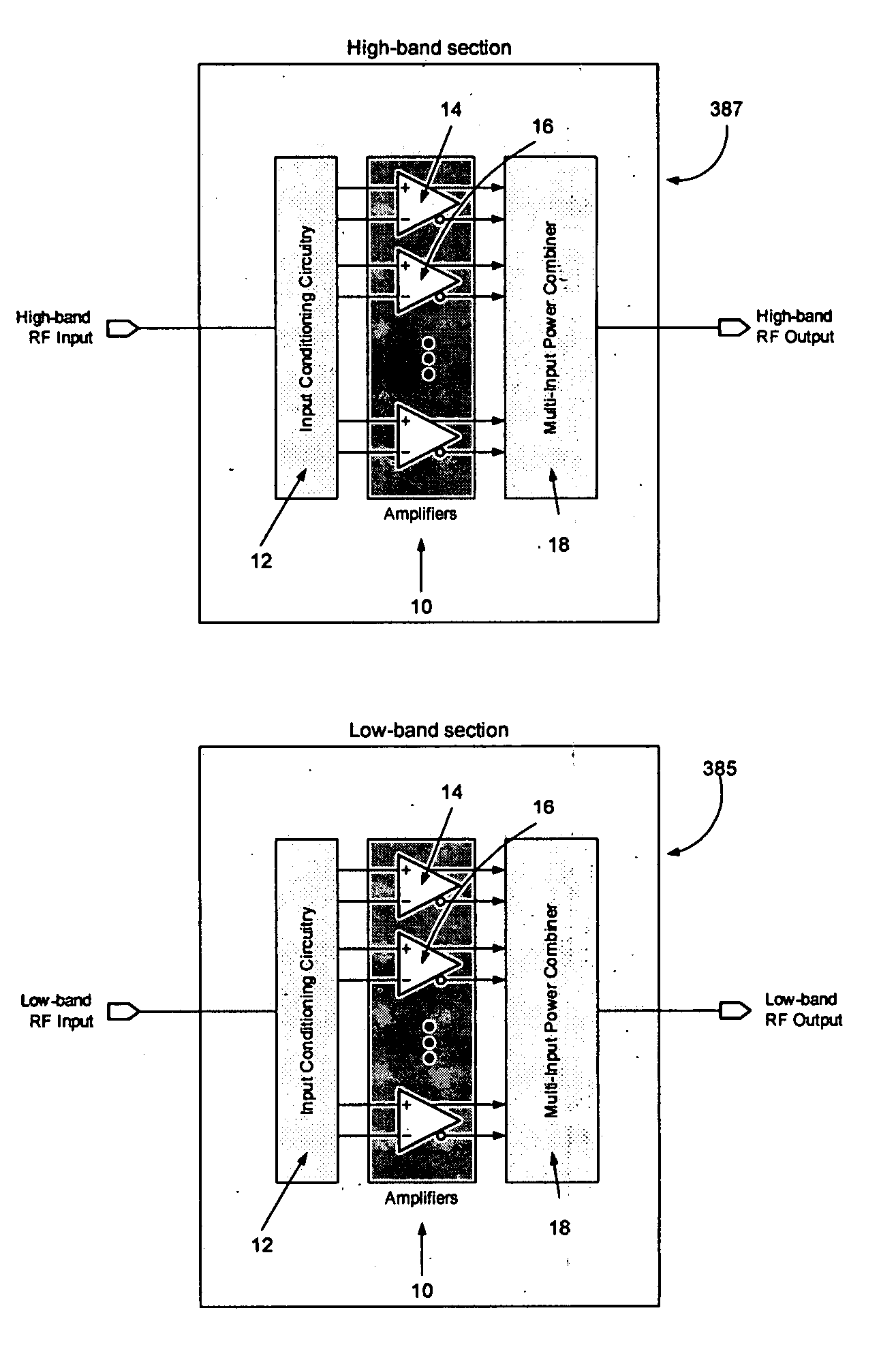
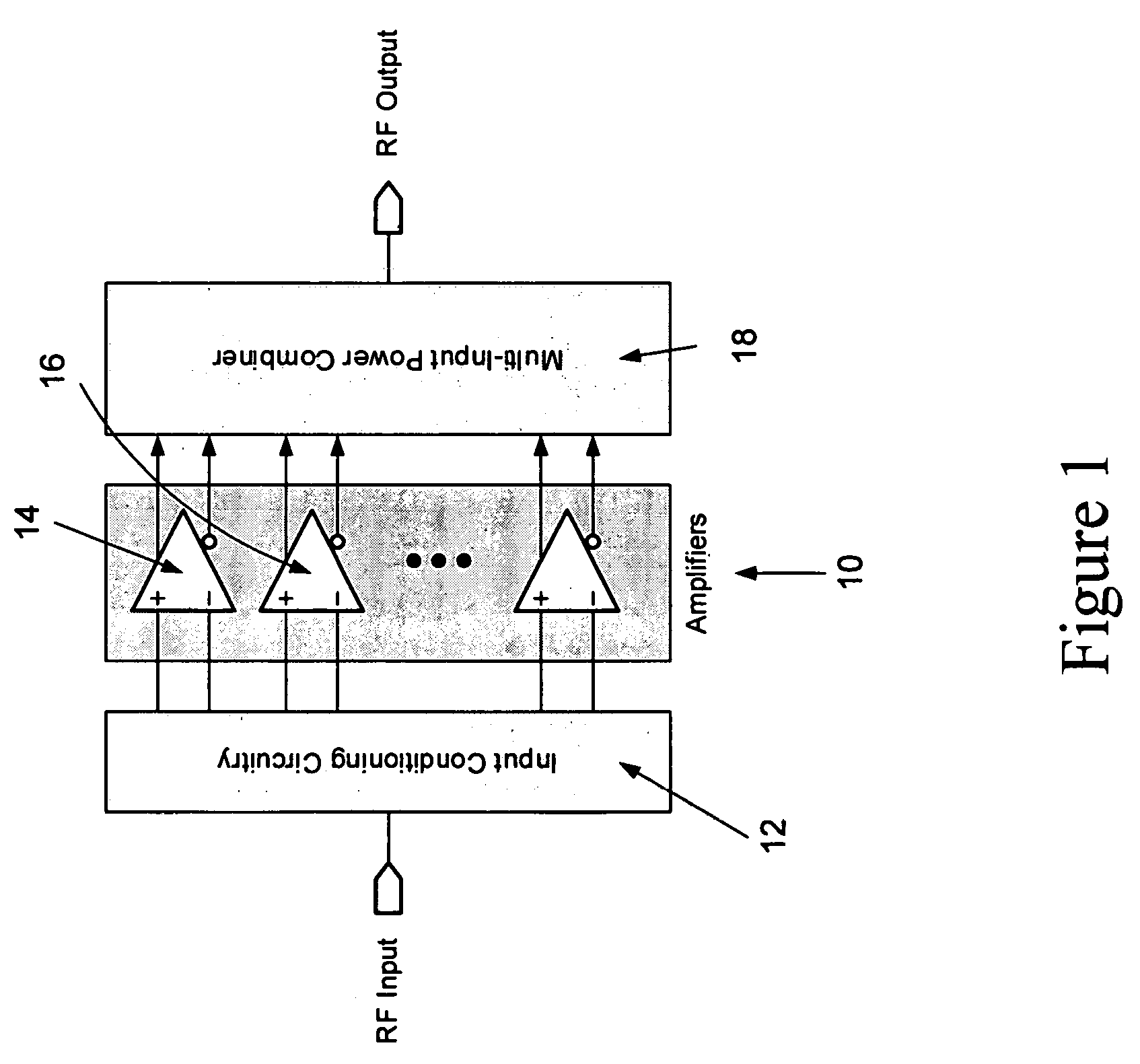
A power amplifier assembly has a first power amplifier with a first input conditioning circuit. At least first and second amplifiers are in parallel with each other and having inputs and outputs. An input signal is coupled to the inputs of the first and second amplifiers. A first multi-input power combiner is provided. The outputs of the at least first and second parallel amplifiers are combined by the first multi-input power combiner to add signals of the outputs constructively. A second power amplifier has a first input conditioning circuit. At least first and second amplifiers are in parallel with each other and having inputs and outputs. An input signal is coupled to the inputs of the first and second amplifiers. A second multi-input power combiner is provided. The outputs of the at least first and second parallel amplifiers are combined by the second multi-input power combiner to add signals of the outputs constructively.

Description

CROSS-REFERENCE TO RELATED APPLICATION[0001]This application claims the benefit of U.S. Ser. No. 60 / 600,316 filed Aug. 9, 2004, and is a continuation-in-part of U.S. Ser Nos. 10 / 887,657, 10 / 888,478 now U.S Pat. No. 7,068,104 and Ser. No. 10 / 888,044, all filed Jul. 8, 2004. All of the applications-referenced applications are incorporated herein by reference.BACKGROUND[0002]1. Field of the Invention[0003]The invention relates generally to power amplifier design and more specifically to radio frequency (RF) power amplifier design.[0004]2. Description of the Related Art[0005]Known power amplifiers, particularly those used with wireless communication devices, face a variety of challenges. For such a power amplifier, the concerns include ensuring sufficient gain, providing efficiency with respect to converting direct current (DC) power to radio frequency (RF) output power, establishing breakdown voltage conditions that are sufficiently high to enable long term use of the device, and achie...

Claims


Application Information

Patent Timeline
Patent Type & Authority Patents(United States)
IPC IPC(8): H03F3/68
CPCH03F3/211H03F3/604H03F2200/534
Inventor BURNS, LAWRENCEWOO, CHONG
Owner QORVO INT PTE LTD
Learn More