Diffusion topography engineering for high performance CMOS fabrication

a technology of cmos and topography engineering, applied in the direction of semiconductor/solid-state device manufacturing, semiconductor devices, electrical equipment, etc., can solve the problems of sti formation process typically creating undesirable divots, reducing the stress of mos devices, and increasing the difficulty of profile control

Active Publication Date: 2008-04-08
TAIWAN SEMICON MFG CO LTD
View PDF15 Cites 34 Cited by
  • Summary
  • Abstract
  • Description
  • Claims
  • Application Information

AI Technical Summary

Benefits of technology

[0013]The DTE modifies the topography of the diffusion regions, thereby improving the stress in the respective MOS device. As a result, device performance is improved.

Problems solved by technology

With the shrinkage of the pitch size of the shallow trench isolation regions and diffusion regions, however, profile control has become more and more challenging.
Conventional MOS device fabrication methods suffer drawbacks.
For example, STI formation processes typically create undesirable divots at the boundary of the STI regions and diffusion regions.
The divots induce reverse narrow channel effects (RNCE) due to parasitic corner transistors and electrical field crowing at edges of the STI regions, leading to corner gate leakage, potential poly gate stringer and gate critical dimension control issues.
Additionally, oxidation processes along sidewalls of the STI regions during the post-gapfill thermal cycle can also induce unfavorable compressive STI stress that significantly degrades device performance at small device widths.
Recessed source / drain regions combined with a stressed CESL may generate favorable strain effects in the channel regions, however, such recesses typically degrade the balance between source / drain resistance and junction depth, and induce potential source / drain-to-substrate leakage due to silicide punch-through.

Method used


Image

  • Diffusion topography engineering for high performance CMOS fabrication
  • Diffusion topography engineering for high performance CMOS fabrication
  • Diffusion topography engineering for high performance CMOS fabrication

Examples


Embodiment Construction

[0019]The making and using of the presently preferred embodiments are discussed in detail below. It should be appreciated, however, that the present invention provides many applicable inventive concepts that can be embodied in a wide variety of specific contexts. The specific embodiments discussed are merely illustrative of specific ways to make and use the invention, and do not limit the scope of the invention.

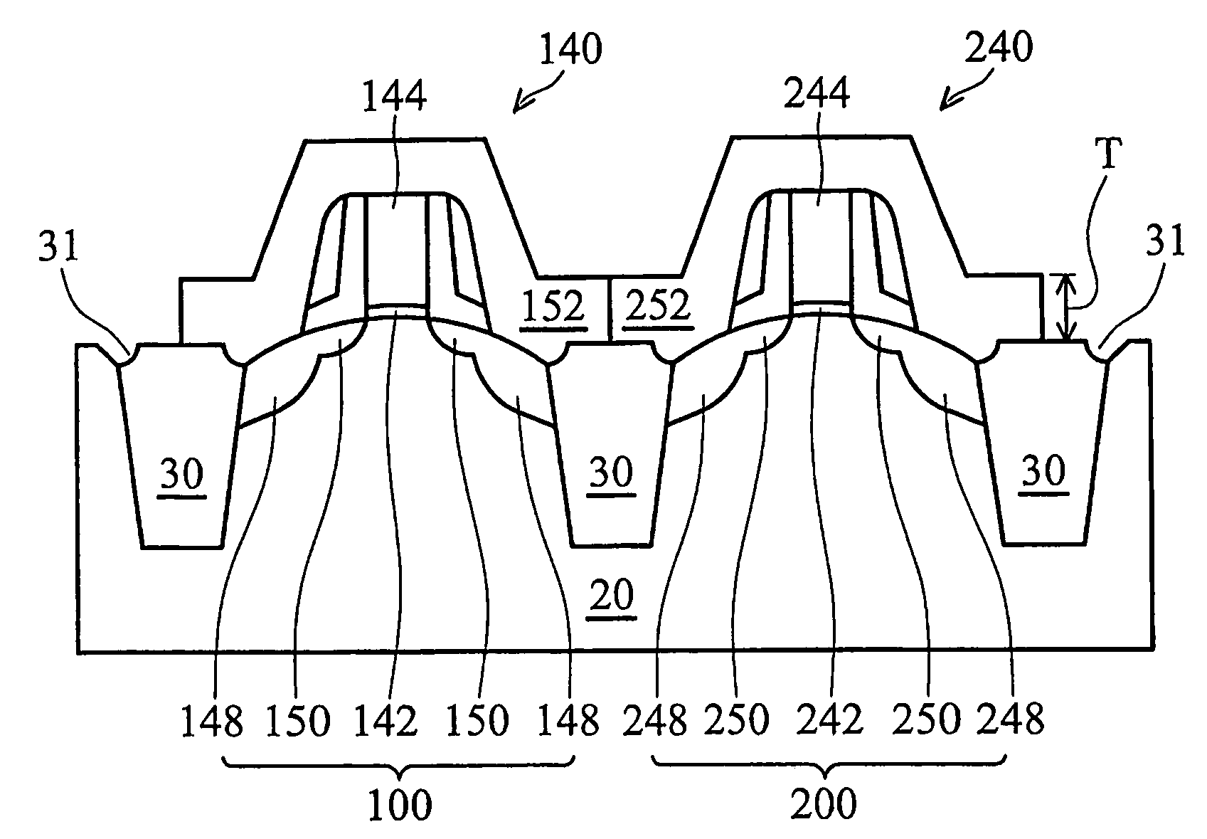
[0020]According to silicon migration theory, hydrogen annealing can reduce the number of dangling bonds of silicon, resulting in migration of surface atoms so as to form a surface with a low surface energy, a reduced surface area and a low stress level. Diffusion topography engineering (DTE), as will be subsequently discussed in the preferred embodiments of the present invention, therefore, can be performed to create favorable topographies for the metal-oxide-semiconductor (MOS) devices. This in turn improves the stress in the channel regions of MOS devices, particularly the ...


PUM


Abstract

Semiconductor structures are formed using diffusion topography engineering (DTE). A preferred method includes providing a semiconductor substrate, forming trench isolation regions that define a diffusion region, performing a DTE in a hydrogen-containing ambient on the semiconductor substrate, and forming a MOS device in the diffusion region. The DTE causes silicon migration, forming a rounded or a T-shaped surface of the diffusion regions. The method may further include recessing a portion of the diffusion region before performing the DTE. The diffusion region has a slanted surface after performing the DTE.

Description

TECHNICAL FIELD[0001]This invention relates generally to structure and fabrication methods of metal-oxide-semiconductor (MOS) devices, and more particularly to performance improvement of the MOS devices through diffusion topography engineering.BACKGROUND[0002]Profile control at the boundary of shallow trench isolation (STI) regions and diffusion regions (or source / drain regions) has been reported to drastically affect metal-oxide-semiconductor (MOS) device characteristics, such as junction capacitance, gate oxide leakage, sub-threshold leakage, junction leakage, etc. Diffusion regions with rounded corners have been proposed to alleviate some of the undesirable effects. With the shrinkage of the pitch size of the shallow trench isolation regions and diffusion regions, however, profile control has become more and more challenging.[0003]Conventional MOS device fabrication methods suffer drawbacks. For example, STI formation processes typically create undesirable divots at the boundary ...

Claims


Application Information

Patent Timeline
Patent Type & Authority Patents(United States)
IPC IPC(8): H01L29/00H01L29/76H01L29/94H01L31/062H01L31/113
CPCH01L21/324H01L21/76224H01L21/823807H01L21/823814H01L21/823878H01L29/1037H01L29/66636H01L29/7834H01L29/7843H01L29/7848
Inventor KO, CHIH-HSINLEE, WEN-CHINKE, CHUNG-HUCHEN, HUNG-WEI
Owner TAIWAN SEMICON MFG CO LTD
Why Eureka
Try Eureka