Reflection type liquid crystal display element, display unit, projection optical system, and projection display system

a liquid crystal display element and display unit technology, applied in the direction of color television details, picture reproducers using projection devices, instruments, etc., can solve the problems of low response speed of display elements, failure to perform proper driving in ordinary driving device substrates of silicon, and high driving voltage. , to achieve the effect of high luminance, high contrast and high luminan

Inactive Publication Date: 2008-02-12
SONY CORP
View PDF41 Cites 3 Cited by
  • Summary
  • Abstract
  • Description
  • Claims
  • Application Information

AI Technical Summary

Benefits of technology

[0028]According to the present invention, although the vertically-aligned liquid crystal layer is less than 2 μm in thickness, the value Δn of the vertically-aligned liquid crystal material is adjusted to be more than 0.1 differently from the conventional recognition, so that the transmissivity of the liquid crystal reaches its saturation with facility at a voltage lower than 5–6V, hence enabling satisfactory driving at a practically low voltage and much enhancing the transmissivity itself. Consequently, it becomes possible to achieve improvements in the reflex vertically-aligned liquid crystal display device having a sufficient transmissivity and superior driving characteristic with low-voltage driving (low required withstand voltage) while holding a high response speed, and also in a display apparatus, a projection optical system and a projection display system using such improved display device.
[0029]The remarkable advantageous functions and effects mentioned above are obtainable due particularly to the selective use of a vertically-aligned liquid crystal material having a value Δn of more than 0.1. In case the liquid crystal layer is reduced in thickness to less than 2 μm for attaining a high response speed, if the directional change of the director is to be affected by the interaction between the orientation film and the liquid crystal molecules, the incident light is prone to be polarized and modulated, since Δn is greater than 0.1, in the liquid crystal in compliance with the applied voltage to eventually cause ready separation of the polarized light, whereby the desired transmissivity can be obtained even at a low voltage.
[0031]According to the above systems, a black level supposed to be proportional to the square of the thickness of the liquid crystal layer can be kept low as the thickness of the vertically-aligned liquid crystal layer is set to less than 2 μm, and therefore a high contrast can be realized even if the F number of the optical unit is less than 3, and yet a high luminance is also attainable with such a small F number. Thus, the projection optical and display systems, each of which is equipped with the reflex liquid crystal device of the invention and an optical unit having an F number under 3, satisfy the requirements for a higher contrast and a higher luminance in comparison with those of any conventional system using the known device and optical unit. The F number of the optical unit is controllable by the focal distance and so forth of a lens used therein.

Problems solved by technology

Recently, one defect of the liquid crystal display device concerning a low response speed thereof is attracting attention as a problem, and it is well known that raising the response speed is an important requisite.
(1) and (2) with reduction of the thickness of the liquid crystal layer, there arises another problem that the driving voltage required for saturating the transmissivity becomes higher. FIG. 15 graphically shows V-T curves obtained by reducing the thickness of the liquid crystal layer in a system using a liquid crystal material (where Δn=0.082) employed in a conventional device, and FIG. 16 graphically shows changes caused in the saturation voltage with the thickness d of the liquid crystal layer.
As described above, if the driving voltage becomes higher in the liquid crystal display device, proper driving fails to be performed in an ordinary driving device substrate of silicon.
It is a matter of course that this problem can be solved by raising the withstand voltage of the pixel driving transistor, but generally the process is complicated with further disadvantages of increasing both the production cost and the power consumption.
Further due to such a rise of the withstand voltage, it is unavoidable that the transistor size is enlarged.
For this reason, it becomes extremely difficult to manufacture high withstand-voltage transistors in a small pixel size (or pitch) less than 10 μm or so in particular.
For the reason mentioned above, it is practically difficult, in any known reflex display device using the conventional vertically-aligned liquid crystal, to reduce the thickness of the liquid crystal layer to less than 2.5 μm.
Reducing the thickness of the liquid crystal layer as described slows down the rise (response speed) to the applied voltage and lowers the yield in manufacture of the device.
Further, in any projection optical system equipped with such known display device, the F number of the optical unit needs to be equal to or greater than 3.5 for maintaining a high contrast as will be explained below, hence bringing another problem that a high luminance is not attained.
However, in the reflex liquid crystal device, generally the black level value (transmissivity in a black state) becomes higher with an increase of the incidence angle, and the polarized-light separation characteristic of the polarized beam splitter is dependent on the angle θ, whereby it is unavoidable that the characteristic is deteriorated with an increase of the angle θ, and the degree of separation into the p-polarized light component and the s-polarized light component is rendered lower when the angular component is great.
Thus, in practical use, there exists a problem of trade-off (difficulty for compatibility) between the luminance and the contrast.
That is, in any projection optical system equipped with the known device, the F number is not settable to less than 3.5 due to a demand for practically realizing a high contrast to a certain degree, hence causing a failure in raising the luminance.

Method used


Image

  • Reflection type liquid crystal display element, display unit, projection optical system, and projection display system
  • Reflection type liquid crystal display element, display unit, projection optical system, and projection display system
  • Reflection type liquid crystal display element, display unit, projection optical system, and projection display system

Examples


embodiment ] 1

[Embodiment]1

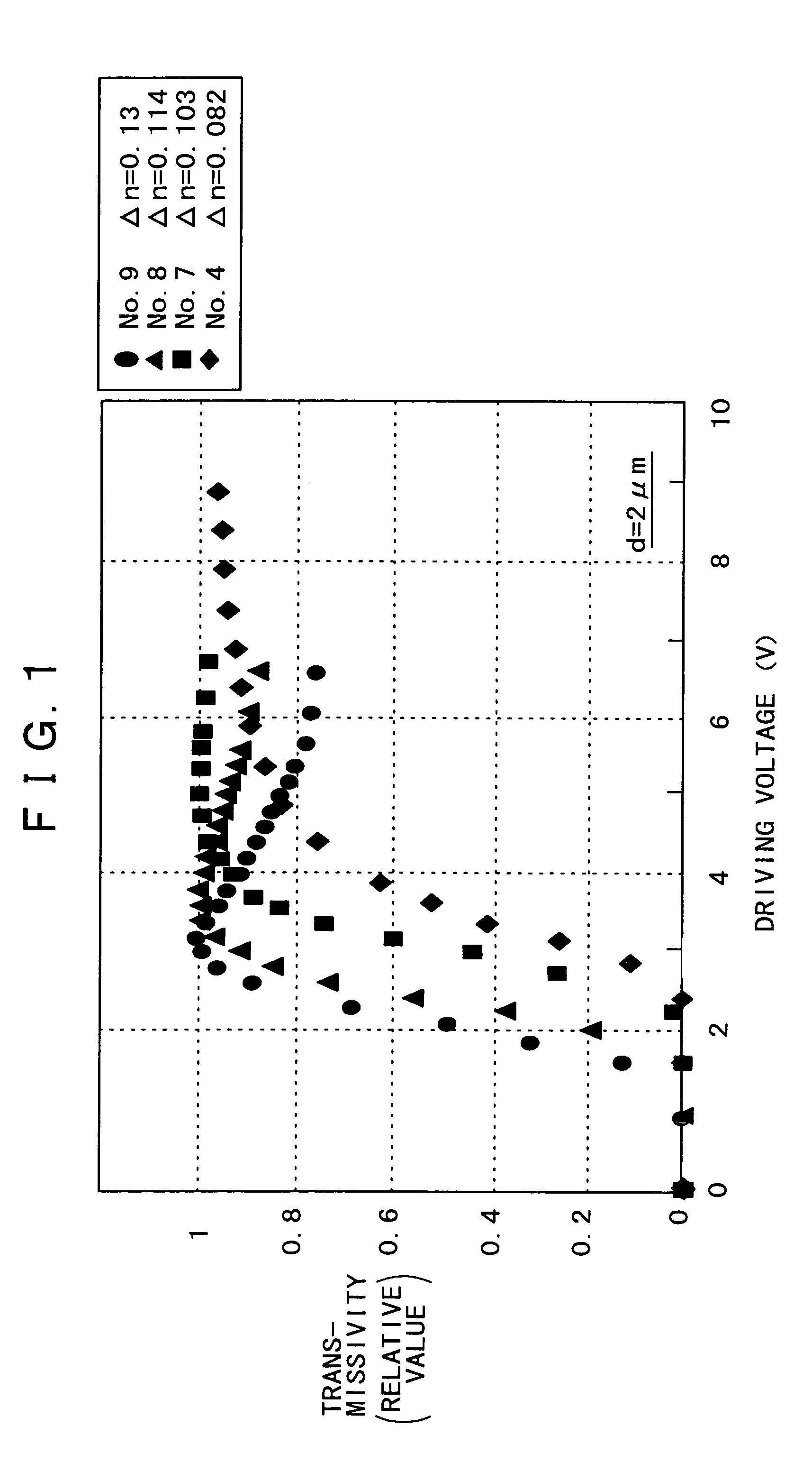
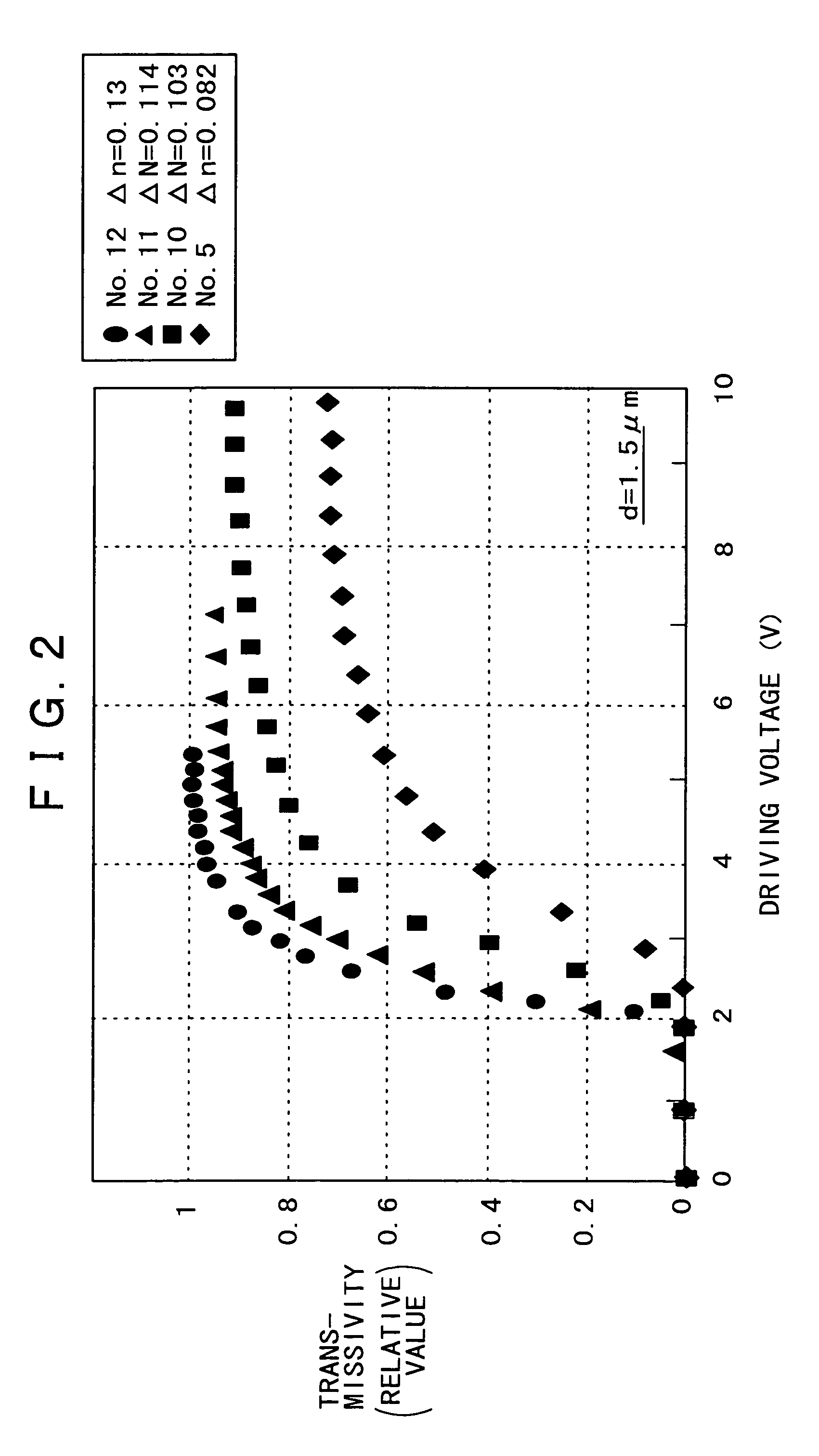
[0092]In the same method as adopted for Comparative example 1 mentioned above, a liquid crystal orientation film of SiO2 was formed on each of a substrate with a transparent electrode and a driving circuit substrate of silicon with an aluminum electrode, and three kinds of vertically-aligned liquid crystal materials (made by Merck Ltd.,) having a negative permittivity anisotropy Δε and a refractive index anisotropy Δn of 0.103, 0.114 and 0.13 were injected between the two substrates to thereby produce nine kinds of reflex liquid crystal display devices (samples Nos. 7–15 in FIG. 5) where the liquid crystal layer thickness (cell gap) was 2 μm, 1.5 μm and 1 μm respectively. The pretilt angle of the liquid crystal was so controlled as to be approximately 2.5°.

[0093]The liquid crystal driving characteristics of the devices thus produced were measured at room temperature similarly to Comparative example 1. FIGS. 1, 2 and 3 graphically show the driving characteristics obtaine...

embodiment ] 2

[Embodiment]2

[0096]The response speed relative to a rise time (from black to white) and a fall time (from white to black) was measured in each of the reflex liquid crystal display devices produced in Embodiment 1. The sum total thereof is regarded as the response speed of each device, and the result is shown in FIG. 5. The measurement was performed at room temperature. FIG. 4 graphically shows the thickness d of the liquid crystal layer as a function with regard to the device having Δn=0.13 as a representative example (samples Nos. 9, 12, 15 with d=2.5 μm in FIG. 5). For comparison, FIG. 4 also shows the response speeds of the known sample No. 1 and the sample produced with d=3 μm (Δn=0.082 in each sample).

[0097]As supposed from Eqs. (1) and (2), the response speed changes substantially in proportion to the square of the thickness of the liquid crystal layer. In the device of the present invention where the layer thickness d is less than 2 μm and Δn is more than 0.1, it was proved t...

embodiment 3

[Embodiment 3]

[0100]The transmissivity (black level) at a zero applied voltage (black state) was measured in the reflex liquid crystal display device produced in Embodiment 1. For systematically examining the black level changes caused in relation to the thickness of the liquid crystal layer, devices having a layer thickness of 3.5 μm (samples Nos. 17–19) were produced with the aforementioned samples of Δn, and also devices having a layer thickness of 2.5 μm were produced similarly, and the black-level transmissivity of each device was measured together with the samples (Nos. 7–15) of Embodiment 1. The respective black level values are graphically shown in FIG. 8 where the numerical values obtained in the devices with a layer thickness of 3.5 μm are indicated as 100% with the individual samples of Δn.

[0101]As shown in FIG. 8, the black level is extremely lowered when the liquid crystal layer becomes thinner than 2 μm in any sample of Δn. In the device with a layer thickness of 1.5 μ...


PUM

PropertyMeasurementUnit
thicknessaaaaaaaaaa
voltageaaaaaaaaaa
thicknessaaaaaaaaaa

Abstract

A superior reflex type vertically-aligned liquid crystal display device wherein the refractive index anisotropy Δn of its liquid crystal material is controlled to be more than 0.1, and the transmissivity of the liquid crystal is saturated with facility at a low voltage below 5 to 6V despite a reduction of the thickness of the vertically-aligned liquid crystal layer to less than 2 μm, hence achieving satisfactory driving at a practically low voltage while attaining another advantage of remarkable improvement in the transmissivity itself. Therefore, the display device indicates a sufficient transmissivity, an excellent low-voltage driving characteristic and a fast response. Further improvements are realizable in a display apparatus, a projection optical system and a projection display system by the use of such display device.

Description

BACKGROUND OF THE INVENTION.[0001]The present invention relates to a reflex liquid crystal (electro-optical) display device adapted for a projection display system or the like, and also to a display apparatus, a projection optical system and a projection display system used in combination with such a display device.[0002]With the recent progress in realizing improved projection display with a high definition, a small size and a high luminance, there are noted and practically utilized reflex display devices which are suited for achieving a dimensional reduction with an enhanced definition and are capable attaining a high optical efficiency.[0003]Out of such display devices, there is reported an active reflex liquid crystal display device wherein a driving element is provided on a silicon substrate which is positioned opposite to a glass substrate having a transparent electrode formed therein and is composed of, e.g., a CMOS (complementary metal oxide semiconductor) circuit, and a dri...

Claims


Application Information

Patent Timeline
Patent Type & Authority Patents(United States)
IPC IPC(8): G02F1/1335G02F1/13G02F1/1337G02F1/1362G02F1/139H04N9/31
CPCG02F1/136277G02F1/1393H04N9/3105H04N9/315H04N9/3197G02F2202/40G02F2203/02G02F1/1337
Inventor HASHIMOTO, SHUNICHIISOZAKI, TADAAKISUGIURA, MINAKO
Owner SONY CORP
Why Eureka
Try Eureka