Correlation detection method and apparatus, transmission diversity detection method and apparatus, each method and apparatus for detection within a small time unit
- Summary
- Abstract
- Description
- Claims
- Application Information
AI Technical Summary
Benefits of technology
Problems solved by technology
Method used
Image
Examples
embodiment 1
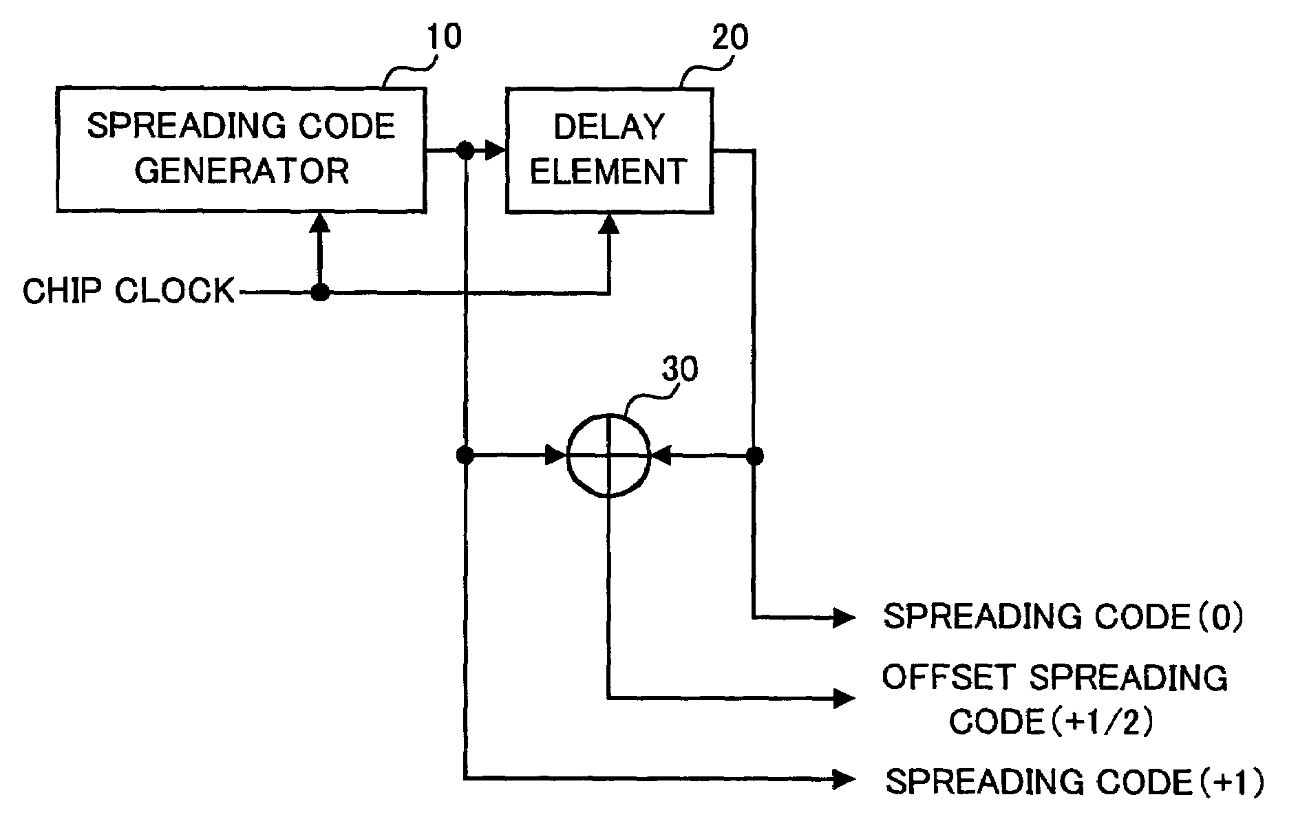
[0037]FIG. 1 is a block diagram showing a configuration of the main part (spreading code generator) of correlation detection apparatus according to claim 1 of the present invention.
[0038]As shown in the figure, spreading code generator 10 generates a spreading code in synchronous with chip clock.
[0039]The spreading code is divided into two sequences, one is given delay corresponding to 1 chip by delay section 20, and the other is just the output without delay.
[0040]Delayed spreading code and non-delayed spreading code are inputted into operation section (logical circuit and combiner) 30. Operator 30 performs interpolation process (combining process), and generates the spreading code which has offset smaller than chip interval (for instance, ½ chip).
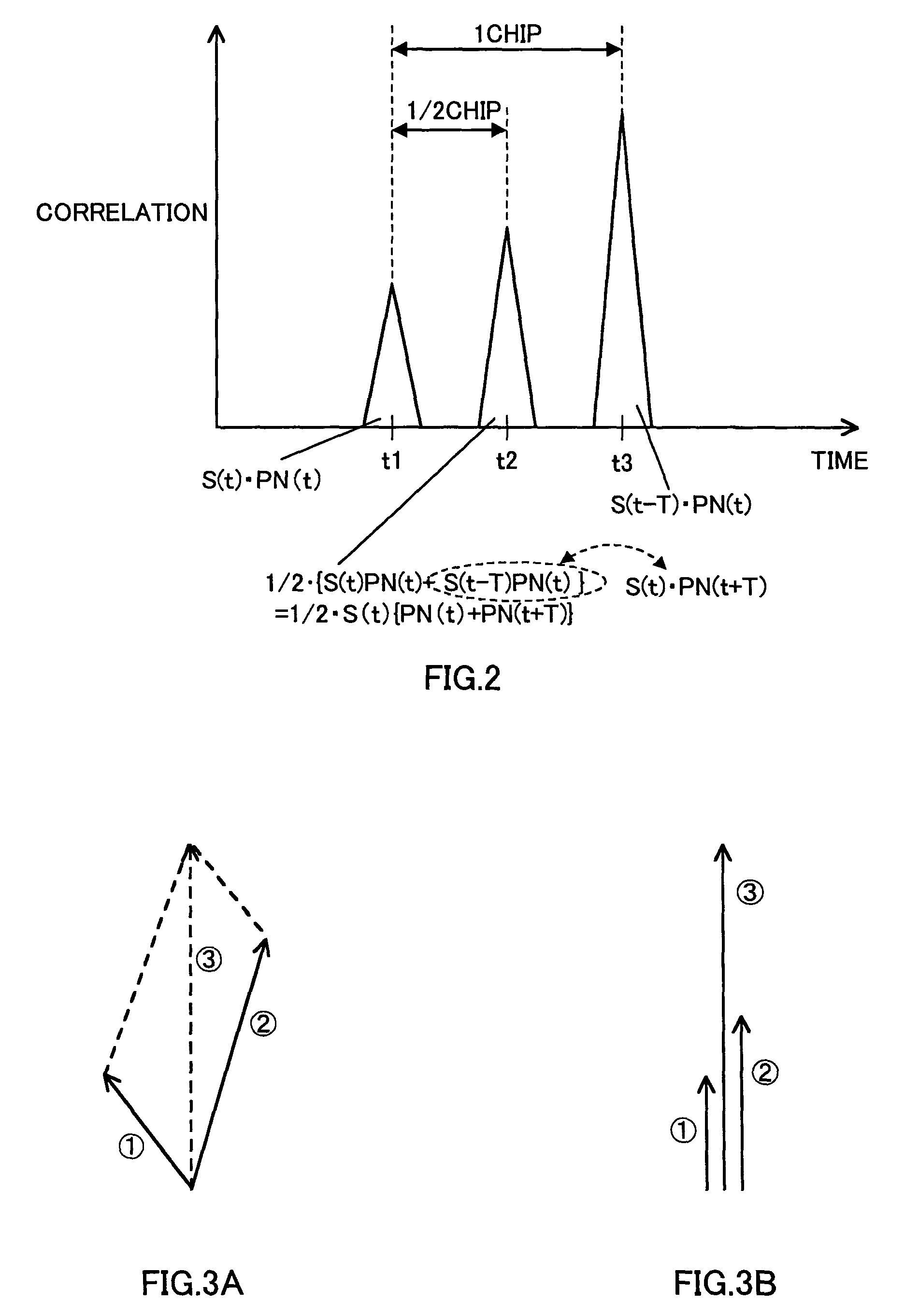
[0041]FIG. 2 is a graph showing the principle of interpolation process (combining process) of the spreading code generated in the circuit of FIG. 1.
[0042]Correlation value of the CDMA reception signal is obtained by multiplying reception ...
embodiment 2
[0073]FIG. 8 is a block diagram showing a configuration of a correlation detection apparatus according to Embodiment 2 of the present invention.
[0074]As shown in FIG. 8, such a correlation detection apparatus comprising computation controller 51, code generator 52, delay elements 53 and 54, adders 55 and 56 to add spreading code of timing close to that outputted from delay elements, spreading code switching section 57 to switch spreading codes based on control signal outputted from computation controller, multiplier 58 to perform multiplication with reception signal, multiplication result switching section 64 to switch the data resulted from accumulation of multiplication results for every spreading code, and integrators 65, 66, and 67 to integrate the accumulated symbol data.
[0075]In the circuit shown in FIG. 8, the employed spreading code and accumulator are switched to be time multiplexed using switch.
[0076]Accordingly, multipliers can be used commonly. Thus, the circuit scale ca...
embodiment 3
[0077]FIG. 9 is a block diagram showing a configuration of a delay locked loop (DLL) according to the present embodiment.
[0078]It is an exemplary circuit which practically uses despreading result of a ±½ chip timing from the aforementioned data combination of neighboring chips.
[0079]As shown in FIG. 9, the DLL of the present embodiment comprising spreading code generator 61, delay elements 62 and 63, adders 64 and 65 to add spreading code of timing close to that outputted from delay elements, multipliers 66, 67 and 68 to carry out multiplication of reception signal, integrators 69, 70, and 71 to integrate the accumulated symbol data from multiplication result, subtractor 75 to subtract the difference of a ±½ chip despreading value, loop filter 74 to fix the time constant of a delay lock loop, and clock generating circuit 73 to carry out clock generation when generation timing outputted from loop filter is changed due to tracking, etc.
[0080]Characteristics of the two inputs of subtra...
PUM
 Abstract
Description
Claims
Application Information
 - R&D
- Intellectual Property
- Life Sciences
- Materials
- Tech Scout
- Unparalleled Data Quality
- Higher Quality Content
- 60% Fewer Hallucinations
Browse by: Latest US Patents, China's latest patents, Technical Efficacy Thesaurus, Application Domain, Technology Topic, Popular Technical Reports.
© 2025 PatSnap. All rights reserved.Legal|Privacy policy|Modern Slavery Act Transparency Statement|Sitemap|About US| Contact US: help@patsnap.com


