
Method to form ultra high quality silicon-containing compound layers

a compound layer, ultra high-quality technology, applied in the direction of chemical vapor deposition coating, semiconductor/solid-state device details, coatings, etc., can solve the problems of cvd reducing throughput, ald being relatively inefficient in speed, and cvd being difficult to achiev

Inactive Publication Date: 2007-11-20
ASM IP HLDG BV
View PDF101 Cites 476 Cited by
  • Summary
  • Abstract
  • Description
  • Claims
  • Application Information

AI Technical Summary

Benefits of technology

This approach enables the production of highly uniform and conformal silicon nitride films with reduced surface roughness and thermal budgets, enhancing manufacturing yields and device reliability by minimizing thickness and compositional variations, and improving insulating properties.

Problems solved by technology

However, as device density continues to increase and geometries continue to become more complicated, deposition processes have been further refined to meet the need for even more uniform and conformal layers.
While ALD gives superior conformality and uniformity in comparison to CVD, ALD is relatively inefficient in terms of speed.
Consequently, while conformality and uniformity is increased, ALD has the drawback of having decreased throughput in comparison to CVD.
Significant variations in the thickness and / or composition of the silicon-containing compound films during the manufacturing process can lead to lower manufacturing yields when the affected devices do not meet the required performance specifications.
Also, variations across the film within a particular device can reduce device performance and / or reliability.
Thus, as substrate sizes increase to accommodate manufacture of larger numbers of microelectronic devices on a circuit, the problems created by the shortcomings of conventional CVD processes also increase.

Method used


Image

  • Method to form ultra high quality silicon-containing compound layers
  • Method to form ultra high quality silicon-containing compound layers
  • Method to form ultra high quality silicon-containing compound layers

Examples


example

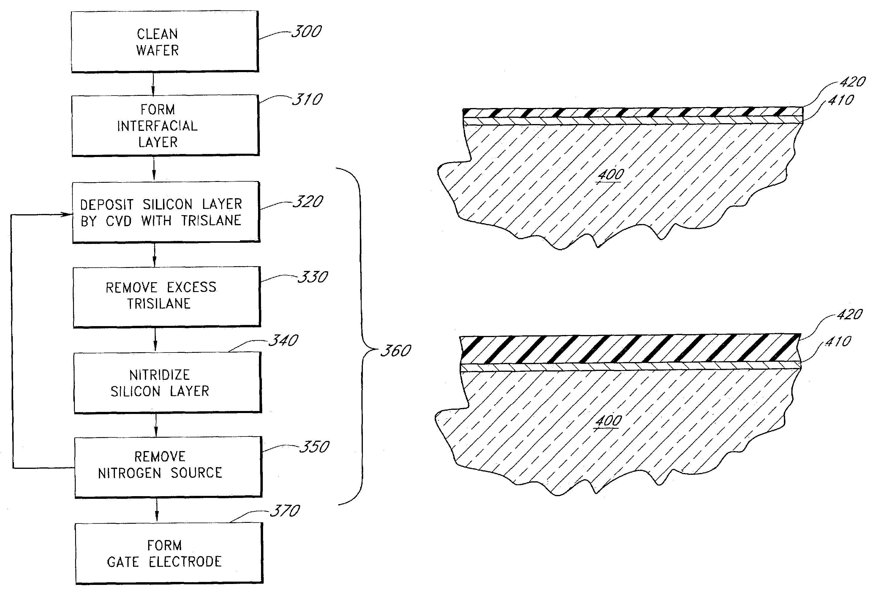
[0151]An exemplary method of forming the illustrated gate structure will now be described in detail:

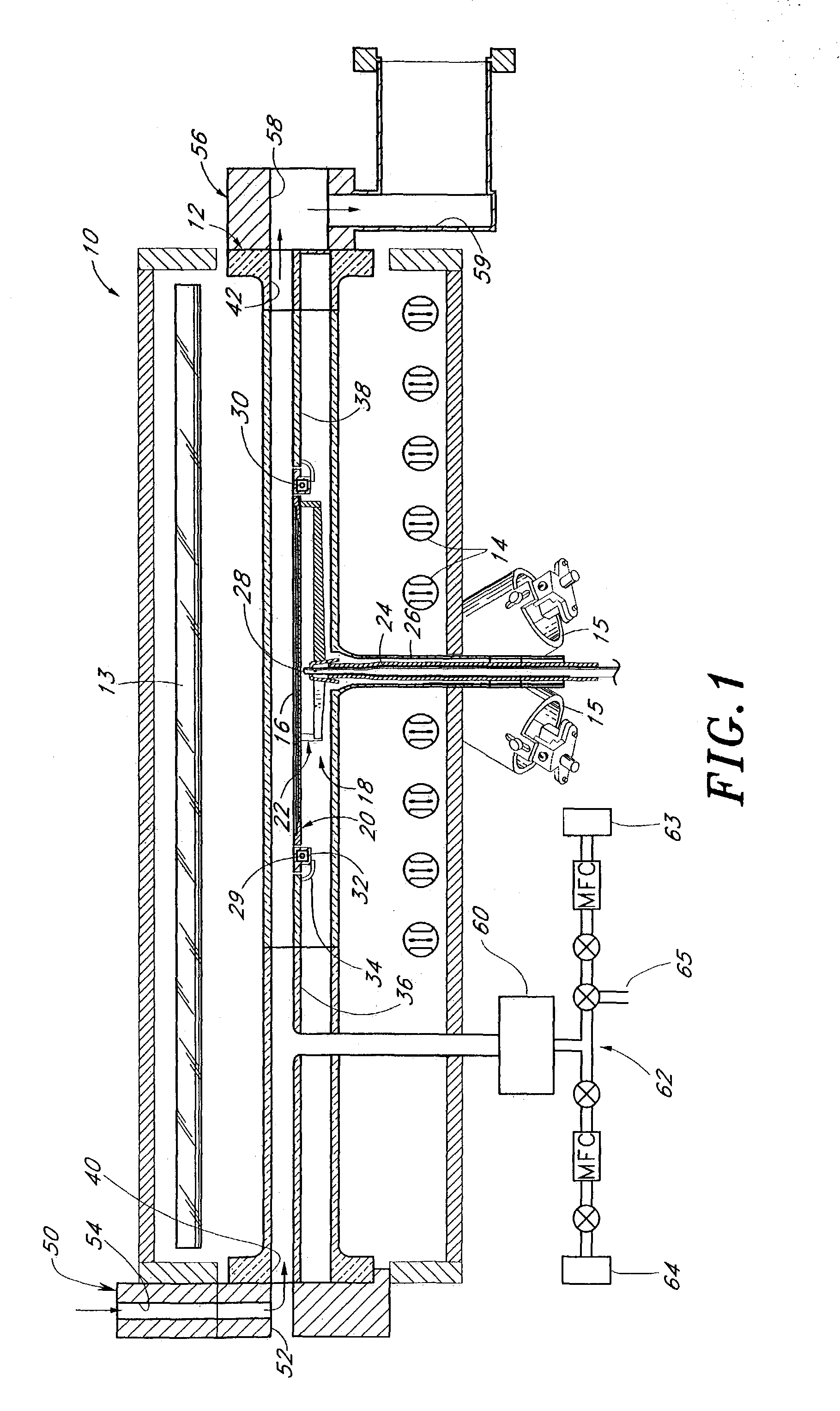
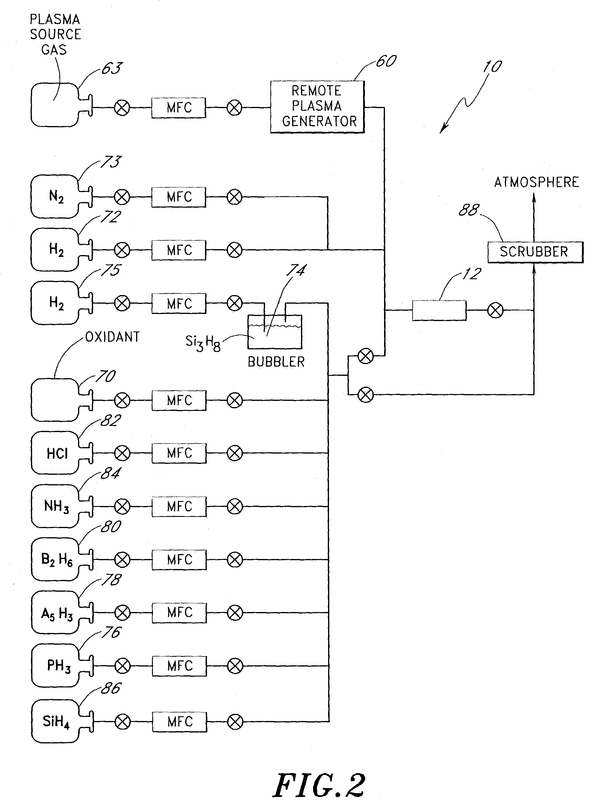
[0152]A silicon nitride layer was formed in a single substrate Epsilon™ reactor from ASM America, Inc. of Phoenix, Ariz. A wafer was loaded into the reaction chamber and prepared for trisilane deposition. Trisilane was flowed into the reaction chamber for 6 seconds at 63 sccm. The reaction chamber was purged for 10 seconds with nitrogen gas. Atomic nitrogen was generated by flowing nitrogen gas into a microwave radical generator (MRG) at 6 slm and flowed into the reaction chamber for 145 seconds. The reaction chamber was then purged with nitrogen gas for 10 seconds. About 5 Å of silicon nitride was deposited per cycle and eight cycles were performed to form a silicon nitride layer of about 40 Å in thickness. Each step of each cycle was performed isothermally at 650° C. and isobarically at 3 Torr.


PUM

PropertyMeasurementUnit
temperatureaaaaaaaaaa

Abstract

Multiple sequential processes are conducted in a reaction chamber to form ultra high quality silicon-containing compound layers, including silicon nitride layers. In a preferred embodiment, a silicon layer is deposited on a substrate using trisilane as the silicon precursor. A silicon nitride layer is then formed by nitriding the silicon layer. By repeating these steps, a silicon nitride layer of a desired thickness is formed.

Description

REFERENCE TO RELATED APPLICATIONS[0001]This application claims the priority benefit of U.S. Provisional Application Ser. No. 60 / 397,576, METHOD TO FORM ULTRA HIGH QUALITY SILICON-CONTAINING LAYERS, filed Jul. 19, 2002. This application is also related to U.S. application Ser. No. 10 / 074,564, THIN FILMS AND METHODS OF MAKING THEM, filed Feb. 11, 2002, and Ser. No. 10 / 074,563, IMPROVED PROCESS FOR DEPOSITION OF SEMICONDUCTOR FILMS, filed Feb. 11, 2002, both of which are hereby incorporated by reference in their entirety.FIELD OF THE INVENTION[0002]This invention relates generally to forming silicon-containing layers during integrated circuit fabrication and, more particularly, to methods for forming uniform silicon compound layers.BACKGROUND OF THE INVENTION[0003]As the dimensions of microelectronic devices become smaller, the physical characteristics of the deposited layers, including uniformity in thickness, composition, and coverage, become more important. This is particularly true...

Claims


Application Information

Patent Timeline
Patent Type & Authority Patents(United States)
IPC IPC(8): H01L21/31H01L21/469C23C16/24C23C16/34C23C16/44C23C16/455C23C16/56H01L21/314H01L21/316H01L21/318
CPCC23C16/24C23C16/345C23C16/45523C23C16/45525C23C16/56H01L21/3185H01L21/02247H01L21/02252H01L21/3144H01L21/31662H01L21/0217H01L21/31612H01L21/0228H01L21/02274H01L21/02164H01L21/02211
Inventor TODD, MICHAEL A.WEEKS, KEITH D.WERKHOVEN, CHRISTIAAN J.POMAREDE, CHRISTOPHE F.
Owner ASM IP HLDG BV
Learn More