Semiconductor memory device

a memory device and semiconductor technology, applied in the direction of information storage, static storage, digital storage, etc., can solve the problems of leak current flow back and difficulty in calculating the readout of memory cells, and achieve the effect of low cos

Active Publication Date: 2007-10-16
XENOGENIC DEV LLC
View PDF7 Cites 20 Cited by
  • Summary
  • Abstract
  • Description
  • Claims
  • Application Information

AI Technical Summary

Benefits of technology

[0026]The present invention has been made in view of the above problems, and it is an object of the present invention to reduce a leak current which depends on a resistance value of a memory cell to be read out and improve a readout margin. It is another object of the present invention to improve a readout margin by a readout circuit in view of an influence of a leak current which depends on a resistance value of a memory cell to be read.
[0027]A semiconductor memory device of the present invention comprises a memory cell array in which a plurality of memory cells consisting of variable resistive elements which store information by a change of electric resistance are arranged in the row direction and the column direction, a plurality of row selection lines extended in the row direction and a plurality of column selection lines extended in the column direction are provided, each of the memory cells in the same row has one end of the variable resistive element connected to the same row selection line, and each of the memory cells in the same column has the other end of the variable resistive element connected to the same column selection line. The semiconductor memory device is characterized by first characteristics in that it comprises a column readout voltage supply circuit which supplies a predetermined first voltage when readout is selected and supplies a predetermined second voltage which is different from the fist voltage when the readout is not selected, to each column selection line, a row readout voltage supply circuit which supplies the second voltage to each row selection line at the time of readout, a sense circuit which detects a current flowing in the selected row selection line separately from a current flowing in the non-selected row selection lines to detect an electric resistance state of the selected memory cell at the time of readout, and in that it further comprises at least either a column voltage displacement prevention circuit which prevents displacement of a supplied voltage level for each of the non-selected column selection lines at the time of readout or a row voltage displacement prevention circuit which prevents displacement of a supplied voltage level for at least the selected row selection line at the time of readout. In addition, the row voltage displacement prevention circuit may prevent displacement of a supplied voltage level for each of the row selection lines at the time of readout.
[0028]According to the first characteristics of the semiconductor memory device, since the displacement of the voltage level of the column selection line is prevented by the column voltage displacement prevention circuit, the leak current induced by the displacement of the voltage level of the column selection line can be reduced, so that a readout margin can be improved. Furthermore, in stead of or in addition to the column voltage displacement prevention circuit, when the row voltage displacement prevention circuit is provided, the leak current induced by the displacement of the voltage level of the row selection line can be reduced, so that the readout margin is further improved. Especially, when both column voltage displacement prevention circuit and row voltage displacement prevention circuit are provided, the readout margin can be improved more effectively.

Problems solved by technology

Thus, when the leak current value is great, it becomes difficult to calculate the memory cell readout currents Id1 and Id2 from the currents IM1 and IM2 measured on the data lines.
There is a problem in which the leak current flows back depending on the resistance value of the selected memory cell even with the method of setting the voltage supplied to the data line and the bit line in FIG. 31, similar to the leak current shown in FIGS. 32 and 33.

Method used


Image

  • Semiconductor memory device
  • Semiconductor memory device
  • Semiconductor memory device

Examples


embodiment 1

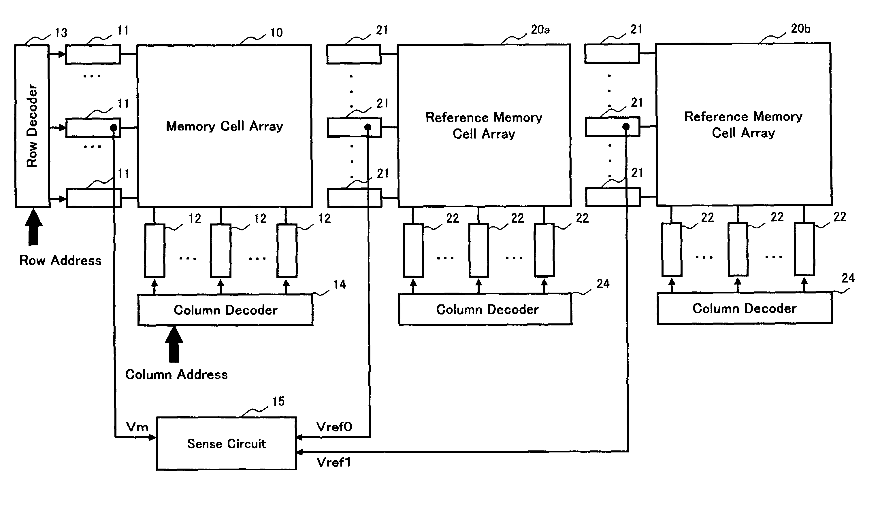
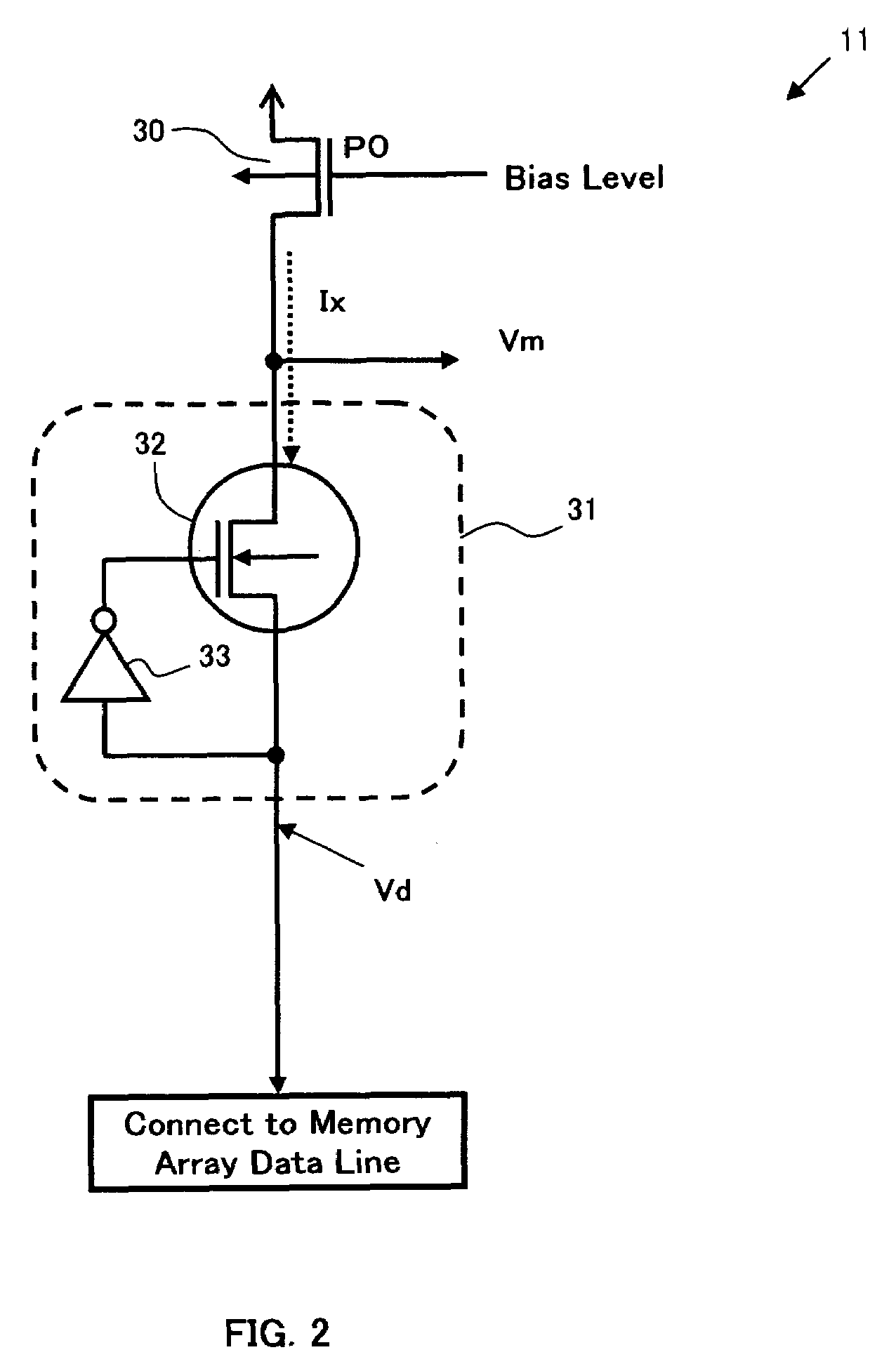
[0072]FIG. 1 is a block diagram showing a main part regarding a readout operation of a memory cell in a memory cell array 10 in the device of the present invention. The memory cell array 10 has a cross-point type of memory cell array structure, in which memory cells (not shown) comprising variable resistive elements which store information by a change of electric resistance are aligned in the form of array in the row and column directions, a plurality of data lines (row selection line) extending in the row direction and a plurality of bit lines (column selection line) extending in the column direction are provided, each memory cell in the same row has one end of the variable resistive element connected to the same data line, and each memory cell in the same column has the other end of the variable resistive element connected to the same bit line. For example, the memory cell array 10 has an array size 16×16 in row and column and in this case, each of the number of data lines and bit...

embodiment 2

[0125]Although the sense circuit 15 having the circuit constitution shown in FIG. 14 is illustrated as the sense circuit of the device of the present invention in the embodiment 1, the sense circuit is not limited to the circuit constitution shown in FIG. 14.

[0126]As shown in FIG. 16, the sense circuit may be consist of one or more stages of inverter circuit 15a. Referring to FIG. 16, the output Vm of the data drive circuit 11 read from a desired memory cell in the memory cell array 10 shown in FIG. 1 is input to the first stage of the inverter circuit 15a of the two-stage inverters. Since this inverter circuit 15a has a voltage amplifying function and a current amplifying function, a general sense amplifier (a circuit which determines binary data on the basis of a reference level and amplifies an output level) can be omitted. In addition, the number of stages of the inverter circuit 15a may be at least one. Here, an inversion level of the first stage inverter of the inverter circui...

embodiment 3

[0131]A third circuit constitution of the sense circuit of the device of the present invention will be described with reference to FIG. 19. According to an embodiment 3, as shown in FIG. 19, a sense circuit 15b comprises a first comparison circuit 16 which compares a voltage level Vm of a selected data line with a first voltage Vref0 which is converted from a first current state in which a current flowing in the selected data line when a high-resistance memory cell is read becomes a maximum level depending on a distribution pattern of an electric resistance state of other non-selected memory cells in a memory cell array, a second comparison circuit 17 which compares the voltage level Vm of the selected data line with a second voltage Vref1 which is converted from a second current state in which a current flowing in the selected data line when a low-resistance memory cell is read becomes a minimum level depending on a distribution pattern of an electric resistance state of other non-...


PUM


Abstract

A semiconductor memory device comprises a column readout voltage supply circuit which supplies a predetermined first voltage when readout is selected and supplies a predetermined second voltage which is different from the fist voltage when the readout is not selected, to each column selection line, a row readout voltage supply circuit which supplies the second voltage to each row selection line at the time of readout, a sense circuit which detects a current flowing in the selected row selection line separately from a current flowing in the non-selected row selection lines to detect an electric resistance state of the selected memory cell at the time of readout, and a column voltage displacement prevention circuit which prevents displacement of a supplied voltage level for each of the non-selected column selection lines at the time of readout.

Description

CROSS REFERENCE TO RELATED APPLICATIONS[0001]This Nonprovisional application claims priority under 35 U.S.C. §119(a) on Patent Applications No. 2004-020749, No. 2004-094057 and 2004-313648 filed in Japan on Jan. 29, 2004, Mar. 29, 2004 and Oct. 28, 2004 respectively, the entire contents of which are hereby incorporated by reference.BACKGROUND OF THE INVENTION[0002]1. Field of the Invention[0003]The present invention relates to a semiconductor memory device having a cross-point type of memory cell array in which memory cells are arranged in the row and column directions, each memory cell in the same row has one end connected to the same row selection line, and each memory cell in the same column has the other end connected to the same column selection line.[0004]2. Description of the Related Art[0005]Recently, development has been progressed for a cross-point type of semiconductor memory device (referred to as the cross-point memory hereinafter) which provides a memory cell array by ...

Claims


Application Information

Patent Timeline
Patent Type & Authority Patents(United States)
IPC IPC(8): G11C7/00G11C7/06G11C7/12G11C11/15G11C7/14G11C8/08
CPCG11C7/06G11C7/062G11C8/08G11C7/14G11C7/12G11C13/0004G11C13/004G11C13/0038G11C13/0023G11C5/14G11C7/1069G11C11/16G11C13/0007G11C13/0016
Inventor INOUE, KOJIMORIKAWA, YOSHINAOSHIMAOKA, ATSUSHITAMAI, YUKIO
Owner XENOGENIC DEV LLC
Why Eureka
Try Eureka