
Fabrication method of light emitting diode package

a technology of light-emitting diodes and fabrication methods, which is applied in the direction of basic electric elements, electrical apparatus, semiconductor devices, etc., can solve the problems of shortening the life of led devices, deteriorating led device properties, and no easy way to the narrow slot b>6/b> in the metal substrate, so as to achieve the effect of convenient application

Active Publication Date: 2007-09-11
SAMSUNG ELECTRONICS CO LTD
View PDF6 Cites 50 Cited by
  • Summary
  • Abstract
  • Description
  • Claims
  • Application Information

AI Technical Summary

Benefits of technology

The present invention provides a fabrication method for LED packages that allows for easier and more precise heat radiation. The method involves preparing a metallic package substrate with a recess and a reflecting surface, selectively anodizing the package substrate to form electrode parts, and mounting a light emitting device on the bottom of the recess. The package substrate can be made by injection molding or press molding of metal. The light emitting device can be connected to the package electrode parts by die bonding or wire bonding. A reflective metal film can be formed on the side surface of the recess before mounting the light emitting device. The method can be applied to bulk production of LED packages.

Problems solved by technology

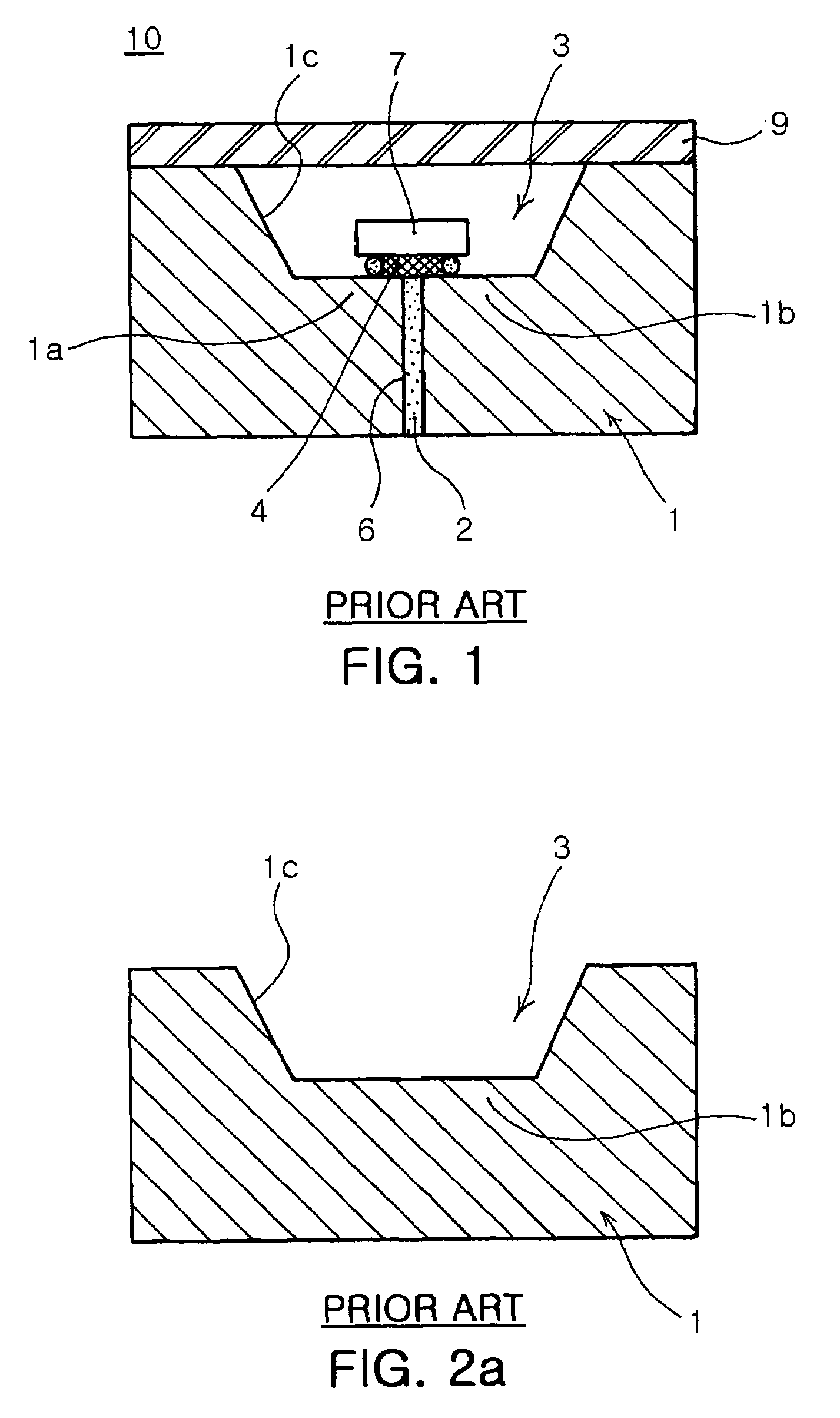
If heat is not efficiently radiated from an LED device, it raises the temperature of the LED device, thereby deteriorating LED device properties while shortening its lifetime.
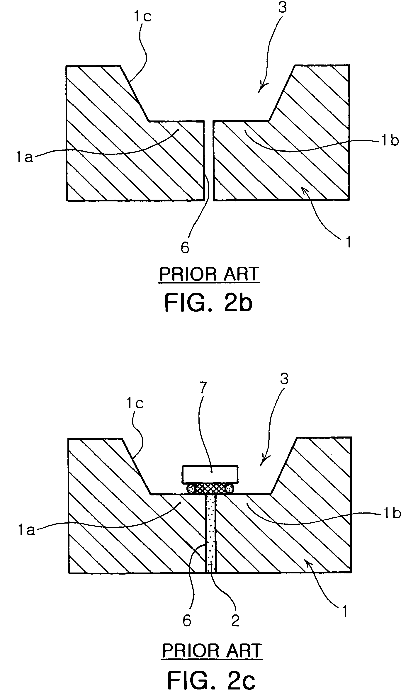
However, there is no easy way to from the narrow slot 6 in the metal substrate by machining or laser processing.
This as a result causes high defective proportion as well as poor yield.

Method used


Image

  • Fabrication method of light emitting diode package
  • Fabrication method of light emitting diode package
  • Fabrication method of light emitting diode package

Examples


Embodiment Construction

[0034]Preferred embodiments of the present invention will now be described in detail with reference to the accompanying drawings. While the present invention will be shown and described in connection with the preferred embodiments, it will be apparent to those skilled in the art that modifications and variations can be made without departing from the spirit and scope of the invention as defined by the appended claims. The embodiments of the present invention are only aimed to provide a full explanation to a person having ordinary skill in the art. Therefore, the shape and size of the elements in the diagrams may be exaggerated for clearer explanation, with the same reference numerals designating the same elements throughout the drawings

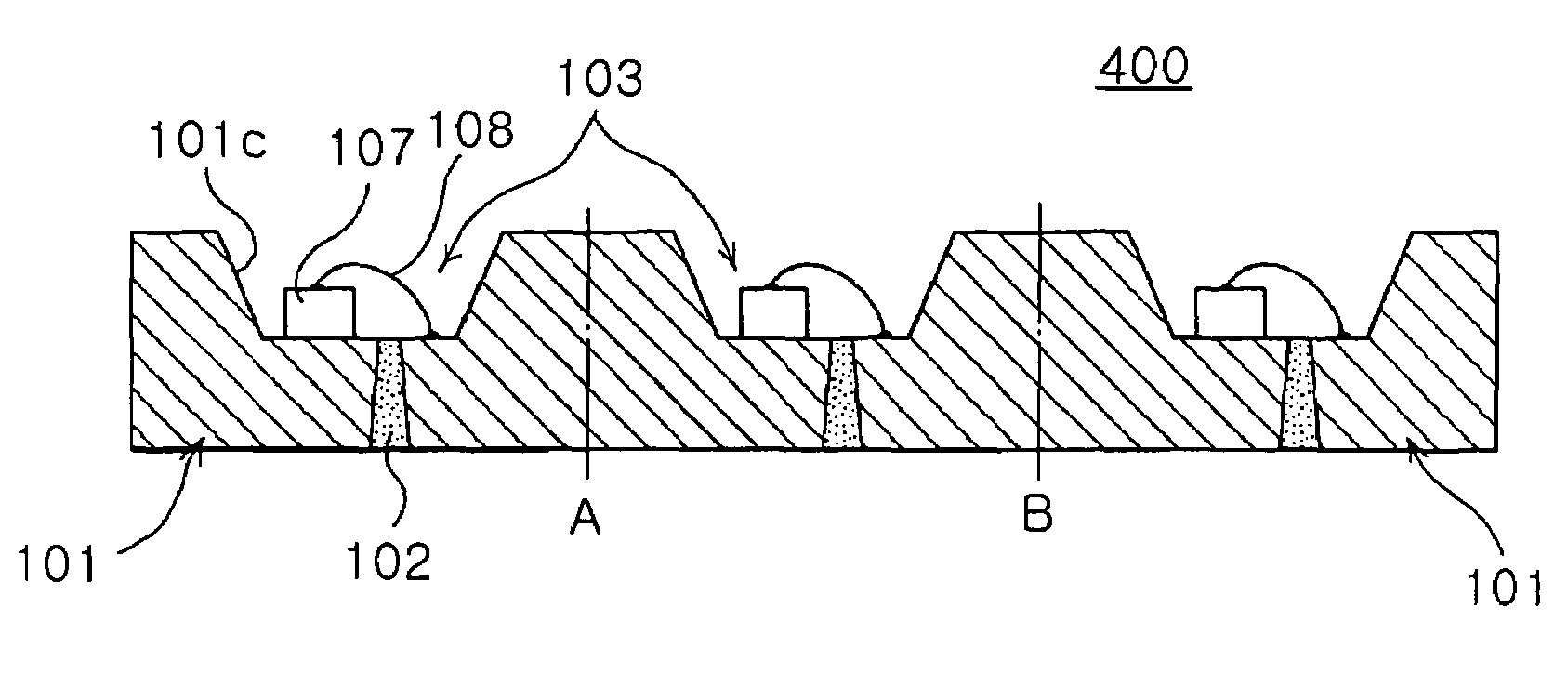
[0035]FIG. 3 is a cross-sectional view illustrating an LED package 100 fabricated according to an embodiment of the invention, and FIG. 4 is a plan view of the LED package 100 shown in FIG. 4. Referring to FIGS. 3 and 4, the LED package 100 includes a...


PUM


Abstract

The invention provides a fabrication method of an LED package for easily fabricating LED packages of excellent heat radiation characteristics. In the method, a metallic package substrate having a recess and a reflecting surface formed in the recess is prepared, and the package substrate is selectively anodized and divided into two package electrode parts divided from each other. Then, an light emitting device is mounted on the bottom of the recess. Preferably, the package substrate is a metal substrate made of Al or Al-based metal.

Description

RELATED APPLICATION[0001]The present application is based on and claims priority from Korean Application Number 2005-36572, filed Apr. 30, 2005, the disclosure of which is hereby incorporated by reference herein in its entirety.BACKGROUND OF THE INVENTION[0002]1. Field of the Invention[0003]The present invention relates to a fabrication method of a light emitting diode package, more particularly, which can achieve excellent heat radiation as well as facilitate mass production.[0004]2. Description of the Related Art[0005]Recent development of Light Emitting Diode (LED) devices made of compound semiconductor material such as GaAs, GaN and AlGaInP has enabled lighting sources of various colors. Decisive factors of LED properties may include color, brightness and optical conversion efficiency. While such LED properties are primarily determined by compound semiconductor material and its internal structure used for an LED device, a package structure for housing the LED device acts as a se...

Claims


Application Information

Patent Timeline
Patent Type & Authority Patents(United States)
IPC IPC(8): H01L21/00H01L33/48H01L33/58H01L33/62H01L33/64
CPCH01L33/486H01L33/647H01L24/97H01L33/62H01L2933/0075H01L2224/48091H01L2924/00014H01L2224/48247H01L2924/01322H01L2924/00H01L2224/16245H01L2924/12041
Inventor LEE, YOUNG KICHOI, SEOG MOONKIM, YONG SIKSHIN, SANG HYUN
Owner SAMSUNG ELECTRONICS CO LTD
Learn More