
Seamless trench fill method utilizing sub-atmospheric pressure chemical vapor deposition technique

a chemical vapor deposition and trench filling technology, applied in the field of microelectronics fabrication, can solve the problems of insufficient film quality of sacvd silicon oxide and its resistance to wet etchant, insufficient step coverage of conventional cvd methods when dealing with high aspect ratio trenches, and inability to meet the requirements of high-quality trenches. , to achieve the effect of eliminating seam defects

Active Publication Date: 2007-07-03
UNITED MICROELECTRONICS CORP
View PDF5 Cites 19 Cited by
  • Summary
  • Abstract
  • Description
  • Claims
  • Application Information

AI Technical Summary

Benefits of technology

The method effectively removes seam defects and densifies the silicon oxide layer, improving film quality and resistance to wet etchants, while maintaining the trench profile integrity.

Problems solved by technology

However, conventional CVD methods have no longer provided satisfactory step coverage when dealing with high aspect ratio trenches, which are typically encountered in the fabrication of advanced integrated circuits.
However, the prior art SACVD techniques have several drawbacks when they are employed in the device isolation field.
First, after the high-temperature anneal treatment, the deposited SACVD film is apt to shrink.
Besides, the film quality of the SACVD silicon oxide and its resistance to wet etchant are not high enough.
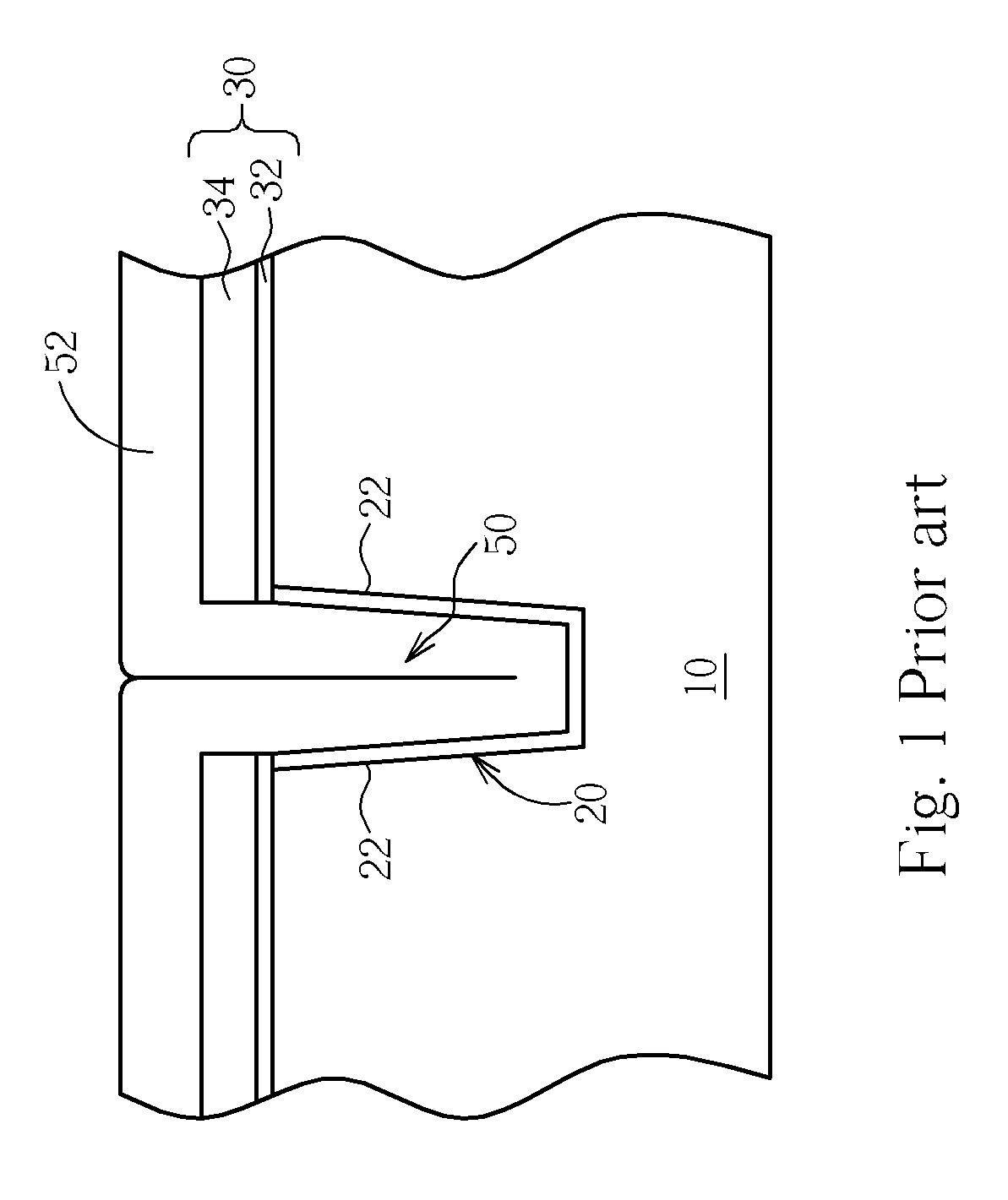
Another problem encountered when employing SACVD to form trench isolation regions is specifically depicted in FIG. 1.
The seam defect 50 is concerned because it cannot be removed by mere high-temperature nitrogen anneal as mentioned supra, and because it is subject to corrosion or attacks by the wet etchant used in the subsequent wet cleaning procedures.

Method used


Image

  • Seamless trench fill method utilizing sub-atmospheric pressure chemical vapor deposition technique
  • Seamless trench fill method utilizing sub-atmospheric pressure chemical vapor deposition technique
  • Seamless trench fill method utilizing sub-atmospheric pressure chemical vapor deposition technique

Examples


Embodiment Construction

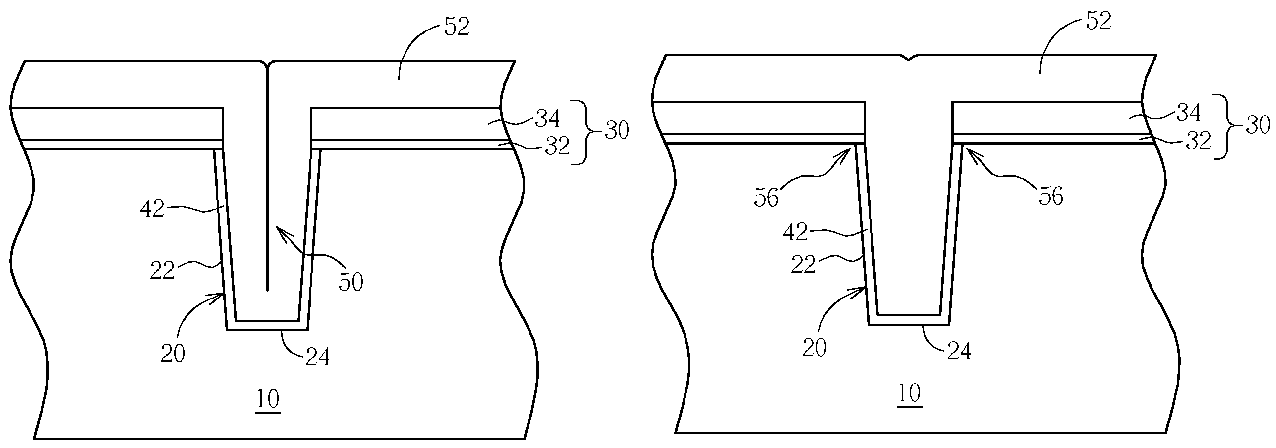
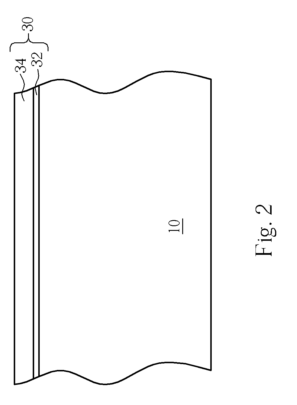
[0016]Please refer to FIG. 2 to FIG. 5. First, as shown in FIG. 2, a pad oxide layer 32 having a thickness of about 30–200 angstroms is formed on a semiconductor substrate 10 such as a silicon substrate. The pad oxide layer 32 may be formed by chemical vapor deposition methods or thermal growth. Subsequently, a silicon nitride pad layer 34 having a thickness of about 500–2000 angstroms is deposited on the pad oxide layer 32. The pad oxide layer 32 and the silicon nitride pad layer 34 serve as a mask layer 30.

[0017]As shown in FIG. 3, conventional lithographic and etching processes are carried out to form an opening 36 in the mask layer 30. The opening 36 exposes a portion of the underlying semiconductor substrate 10. Using the mask layer 30 as an etching hard mask, the exposed semiconductor substrate 10 is etched through the opening 36, thereby forming a trench 20 having a trench depth of about 3500–6000 angstroms. This invention is particularly suited for the trench 20 that has an ...


PUM

PropertyMeasurementUnit
temperatureaaaaaaaaaa
volumetric flowrate ratioaaaaaaaaaa
temperatureaaaaaaaaaa

Abstract

A seamless trench fill method utilizing ozone-assisted sub-atmospheric pressure chemical vapor deposition (SACVD) technique is provided. After the deposition of a SACVD silicon oxide film, the substrate is subjected to a steam anneal that is performed under H2 / O2 environment at a relatively lower temperature ranging between 500° C. and 800° C. for a time period of no less than 30 minutes. The seam defect in the trench is effectively eliminated by this low-temperature steam anneal. To densify the SACVD silicon oxide film, a subsequent N2 anneal is carried out at a higher temperature, for example, 1050° C.

Description

BACKGROUND OF INVENTION[0001]1. Field of the Invention[0002]The present invention relates to the field of microelectronics fabrication and, more particularly, to a seamless trench-fill process utilizing sub-atmospheric pressure chemical vapor deposition (SACVD) technique.[0003]2. Description of the Prior Art[0004]Trench isolation techniques such as shallow trench isolation (STI) processes are known in the art. Generally, to form an STI isolation region on a substrate, a recess is first etched into the substrate, and then filled with an insulating dielectric film, which is typically a CVD silicon oxide film. Subsequently, a chemical mechanical polishing (CMP) process is carried out to provide a planar surface.[0005]As the critical dimension of the integrated circuit devices shrinks to very deep sub-micron scale or beyond, it becomes more and more critical to fabricate reliable and effective device isolation in the art. However, conventional CVD methods have no longer provided satisfa...

Claims


Application Information

Patent Timeline
Patent Type & Authority Patents(United States)
IPC IPC(8): H01L21/76
CPCH01L21/76224
Inventor HSU, SHAO-TACHEN, NENG-KUOTSAI, TENG-CHUN
Owner UNITED MICROELECTRONICS CORP
Learn More