Semiconductor package having an optical device and a method of making the same

a technology of semiconductor devices and optical devices, which is applied in the direction of semiconductor devices, semiconductor/solid-state device details, electrical apparatus, etc., can solve the problems of limited application and unsuitable packaging of optical devices, and achieve the effect of simple method

Active Publication Date: 2007-06-12
ADVANCED SEMICON ENG INC
View PDF8 Cites 7 Cited by
  • Summary
  • Abstract
  • Description
  • Claims
  • Application Information

AI Technical Summary

Benefits of technology

[0007]The objective of the invention is to provide a semiconductor package having an optical device and a method of making the same, which is suitable for packaging an optical device. The process of the method is simple and cost-saving.

Problems solved by technology

However, in the case that the chip 20 is an optical device, its active surface must be capable of receiving light, and the technology disclosed in the patent is not suitable for packaging an optical device.
Therefore, the field of application is limited.

Method used


Image

  • Semiconductor package having an optical device and a method of making the same
  • Semiconductor package having an optical device and a method of making the same
  • Semiconductor package having an optical device and a method of making the same

Examples


Embodiment Construction

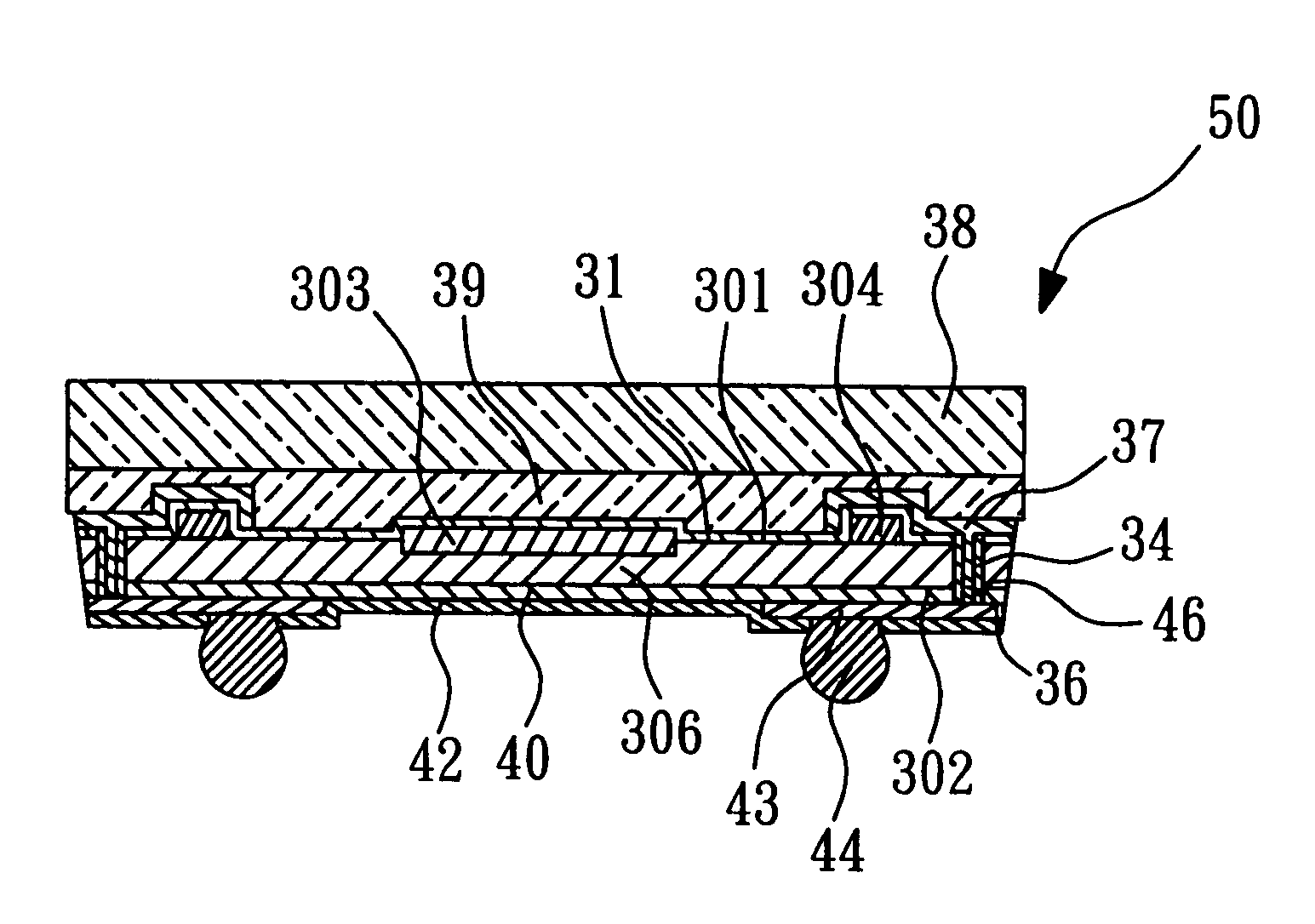
[0023]Referring to FIG. 5, the flow chart of the method of packaging the semiconductor package having an optical device according to the preferred embodiment of the present invention is shown. FIGS. 6 to 23 are schematic views corresponding to the steps in FIG. 5.

[0024]Firstly, in step S101, a wafer 30 is provided. The wafer 30 has an active surface 301, a back surface 302, and a plurality of sawing lines 305. The active surface 301 has at least one upper pad 304 and an optical device 303 thereon, wherein the optical device 303, for example, a Complementary Metal-Oxide Semiconductor (CMOS), is electrically connected to the upper pad 304. A plurality of chips 306 are defined by the sawing lines 305 as shown in FIG. 6.

[0025]Then, in step S102, a dielectric layer 31 is formed on the active surface 301 of the wafer 30, as shown in FIG. 7. The dielectric layer 31 is formed to enable a following metal layer to be formed more easily on the active surface 301 of the wafer 30. Therefore, thi...


PUM


Abstract

The present invention relates to a semiconductor package having an optical device and a method of making the same. The package comprises a chip, an upper metal redistribution layer, a transparent insulating layer, and a lower metal redistribution layer. The chip has an active surface, a back surface, at least one through hole, an optical device, and at least one upper pad, wherein the optical device is electrically connected to the upper pad, and the through hole is filled with a metal post. An insulating layer is disposed between the wall of the through hole and the metal post. The upper metal redistribution layer is disposed on the active surface of the chip, and is used for connecting the upper pad and the metal post. The transparent insulating layer is disposed on the active surface of the wafer. The lower metal redistribution layer is disposed on the back surface of the chip, and is connected to the metal post. Whereby, the optical device is packaged, and the manufacturing process is simplified, and the cost is reduced.

Description

BACKGROUND OF THE INVENTION[0001]1. Field of the Invention[0002]The invention relates to a semiconductor package and a method of making the same, and more particularly, to a semiconductor package having an optical device and a method of making the same.[0003]2. Description of the Related Art[0004]Referring to FIGS. 1 and 2, a conventional package and a conventional method of making the same are disclosed in U.S. Pat. No. 6,040,235. The conventional method of packaging the package 10 is described as follows. Firstly, an insulating material 11 is attached to the active surface of a wafer. Then, the wafer is sawed into a plurality of dies 12 and the pads 13 are exposed on the active surfaces of the dies 12. Then, a plurality of electrical contacts 16 are formed after two insulating layers 14, 15 are formed on the lower surface of the dies 12. One end of each of the electrical contacts 16 is connected to the pad 13, and each electrical contact 16 extends to the upper surface 112 of the ...

Claims


Application Information

Patent Timeline
Patent Type & Authority Patents(United States)
IPC IPC(8): H01L21/00
CPCH01L23/3114H01L24/94H01L23/3107H01L21/78H01L2224/0401H01L23/525H01L2224/0231H01L2224/02372H01L2224/13022H01L2224/13024H01L2224/274H01L2224/82039H01L2924/01005H01L2924/01006H01L24/03H01L24/05H01L24/11H01L24/13H01L2224/11334H01L2224/94H01L2224/131H01L2224/11H01L2224/03H01L2924/014
Inventor FENG, YAO-HSIN
Owner ADVANCED SEMICON ENG INC
Why Eureka
Try Eureka