
Semiconductor fabrication process, lateral PNP transistor, and integrated circuit

a lateral pnp transistor and semiconductor technology, applied in the field of silicon ic technology, can solve the problems of low gain (beta), not suitable for all applications, and lack of good pnp-transistors in bipolar-only rf-ic processes, and achieve the effect of reducing contact resistance and reducing the recombination rate of emitters

Inactive Publication Date: 2007-05-15
INFINEON TECH AG
View PDF9 Cites 10 Cited by
  • Summary
  • Abstract
  • Description
  • Claims
  • Application Information

AI Technical Summary

Benefits of technology

The present invention provides a method for fabricating an integrated circuit with a lateral PNP transistor that overcomes previous problems. The method includes forming a p-type doped substrate, adding a buried n+-type doped region for a PMOS transistor structure, adding an n-type doped region above the buried n+-type doped region, adding field isolation areas around the n-type doped region, adding a PMOS gate region, adding a diffused n+-type doped contact from the upper surface of the substrate to the buried n+-type doped region, and connecting the PMOS transistor structure to resemble a PNP transistor. The method also includes forming a lateral PNP transistor in an integrated circuit, which includes a p-type doped semiconductor substrate, a PMOS transistor structure, and a diffused n+-type doped region connected to the substrate by a diffused n+-type doped contact. The invention provides a more efficient and reliable method for fabricating integrated circuits with lateral PNP transistors.

Problems solved by technology

The versatility of a BiCMOS process is many time preferred, although it is not suited for all applications.
However, a bipolar-only RF-IC process usually lacks good PNP-transistors, since the process is commonly designed for optimal vertical NPN transistor performance.
A primary problem with the lateral PNP devices made by using MOS transistors is the low gain (beta), which typically is lower than 10.
Another problem is the comparatively large area occupied by each device.

Method used


Image

  • Semiconductor fabrication process, lateral PNP transistor, and integrated circuit
  • Semiconductor fabrication process, lateral PNP transistor, and integrated circuit
  • Semiconductor fabrication process, lateral PNP transistor, and integrated circuit

Examples


Embodiment Construction

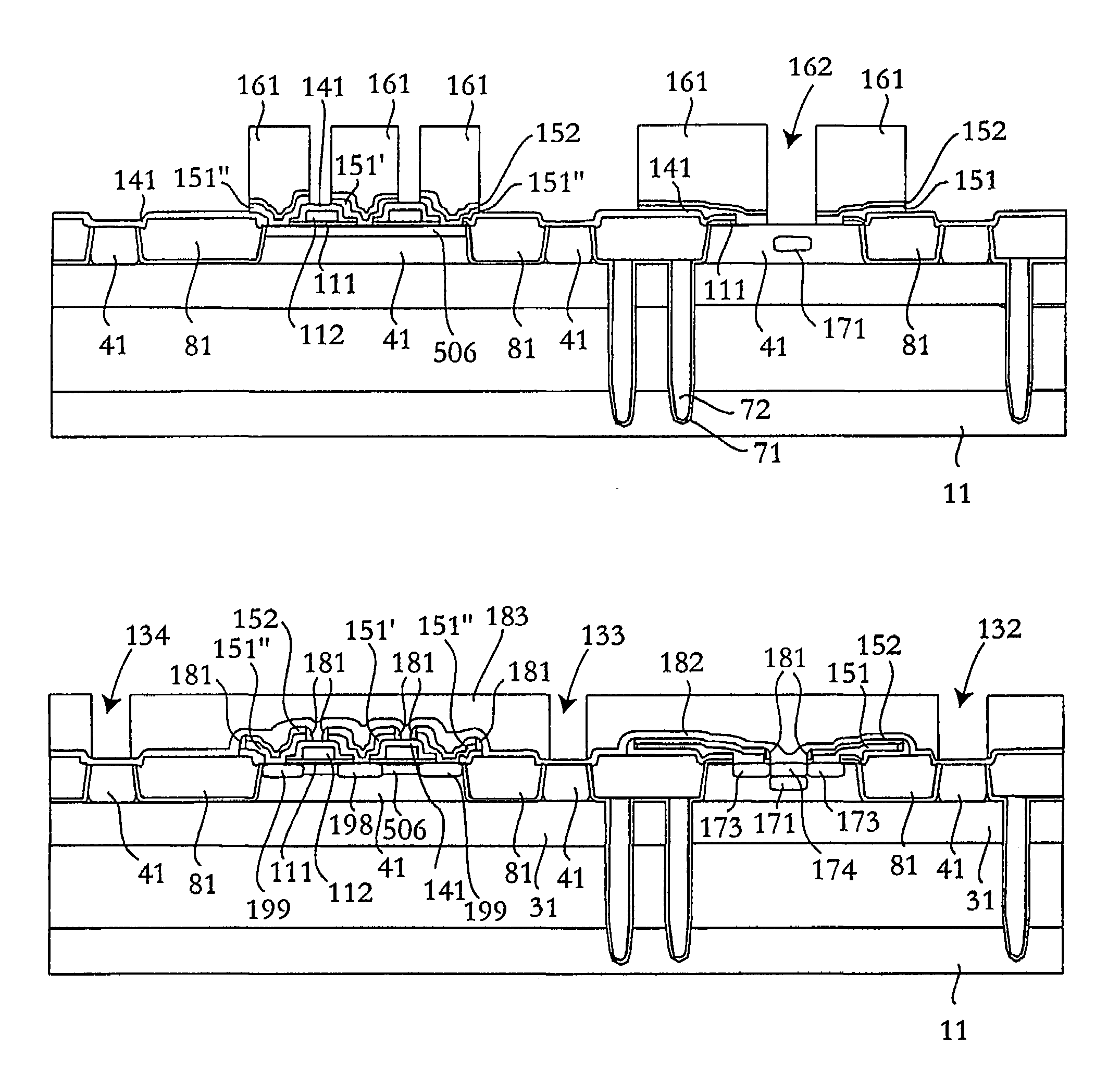
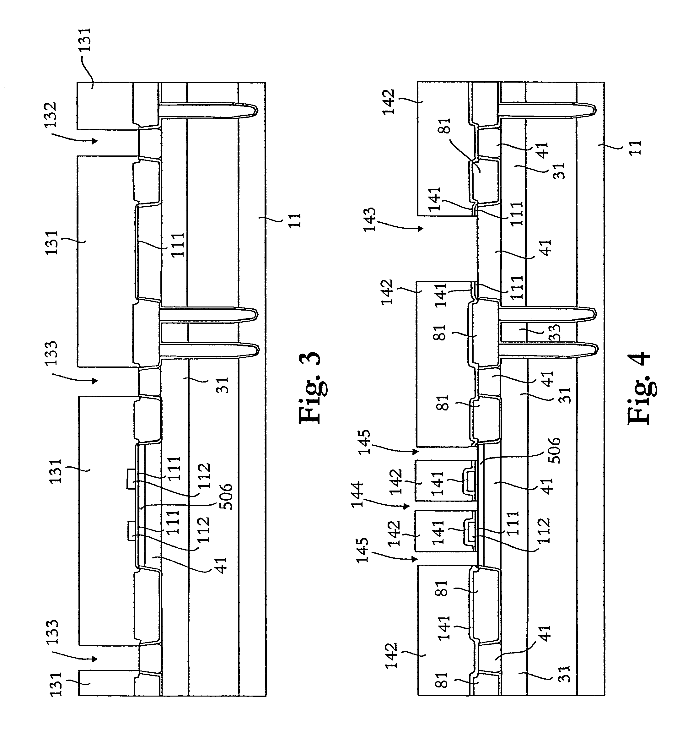
[0029]A process of manufacturing a PMOS-based lateral PNP transistor in a bipolar process, to which only a few process steps are added, is described below. To illustrate the process, a description of simultaneous formation of a vertical bipolar NPN transistor is also included.

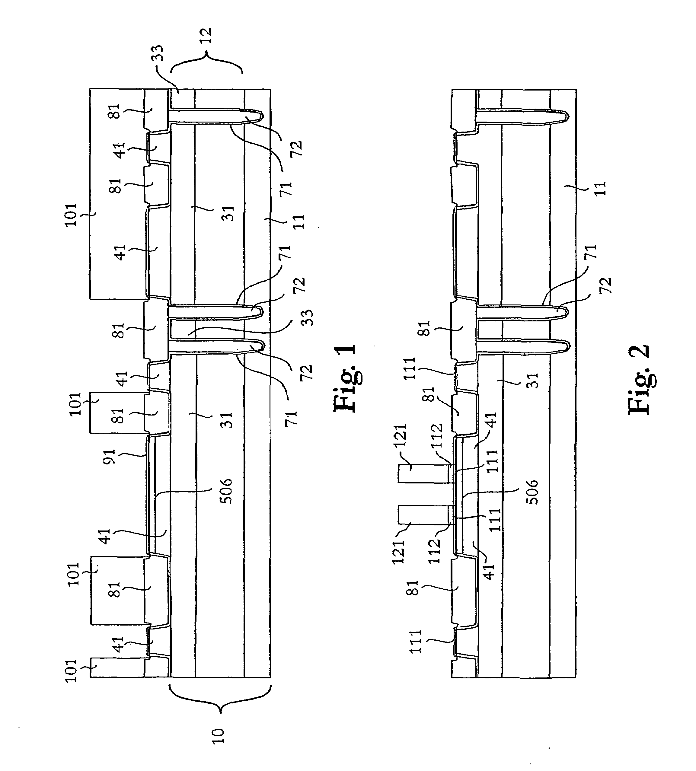
[0030]To reach a structure as the one illustrated in FIG. 1 a starting material 10 consisting of a highly p+-doped wafer 11 is provided, on which a low-doped silicon layer 12 of p-type is grown. Alternatively, the p-type wafer can be a homogeneously low-doped p-type wafer (not illustrated).

[0031]In the surface layer 12 buried n-doped 31 and p-doped 33 regions are formed by means of (i) forming a thin protective layer of silicon dioxide on the layer 12; (ii) forming a mask thereon by photolithographic methods to define areas for a PMOS structure, and the bipolar transistor, respectively; (iii) n+-type doping the areas defined by the mask; (iv) removing the mask; (v) heat treating the structure obtained; (vi) opt...


PUM


Abstract

A method in the fabrication of an integrated bipolar circuit comprises the steps of: providing a p-type substrate; forming in the substrate a buried n+-type region and an n-type region above the buried n+-type region; forming field isolation areas around the n-type region; forming a PMOS gate region on the n-type region; forming a diffused n+-type contact from the upper surface of the substrate to the buried n+-type region; the contact being separated from the n-type region; forming a p-type polysilicon source on the n-type region; forming a p-type source in the n-type region; forming a p-type drain in the n-type region; and connecting the PMOS transistor structure to operate as a PNP transistor, wherein the source is connected to the gate and constitutes an emitter of the PNP transistor; the drain constitutes a collector of the PNP transistor; and the n-type region constitutes a base of the PNP transistor.

Description

CROSS REFERENCE TO RELATED APPLICATION[0001]This application is a continuation of copending International Application No. PCT / SE03 / 00221 filed Feb. 11, 2003 which designates the United States, and claims priority to Swedish application no. 0200414-1 filed Feb. 13, 2002.TECHNICAL FIELD OF THE INVENTION[0002]The present invention generally relates to the field of silicon IC-technology, and more specifically the invention relates to a fabrication method of a lateral PNP transistor in a semiconductor process flow, especially designed for bipolar RF-IC:s, to a lateral PNP transistor, and to an integrated circuit including the transistor.DESCRIPTION OF RELATED ART AND BACKGROUND OF THE INVENTION[0003]Advanced silicon bipolar, CMOS or BiCMOS circuits are used today for high-speed applications in the 1–5 GHz frequency range, replacing circuits previously only possible to realize using III–V based technologies.[0004]A common trend in microelectronics is to integrate more and more functions o...

Claims


Application Information

Patent Timeline
Patent Type & Authority Patents(United States)
IPC IPC(8): H01L21/8238H01L21/331H01L21/8249H01L27/06H01L29/735
CPCH01L21/8249H01L27/0623H01L29/6625H01L29/735
Inventor NORSTROM, HANSJOHANSSON, TED
Owner INFINEON TECH AG
Learn More