
Complementary MIS device

a technology of mis-matching and semiconductors, applied in the direction of semiconductor devices, electrical apparatus, transistors, etc., can solve the problems of affecting the operation speed of semiconductor devices, increasing power consumption, and difficulty in wafer handling, so as to achieve the effect of balancing the current drivability

Inactive Publication Date: 2007-04-10
TOHOKU UNIV
View PDF16 Cites 12 Cited by
  • Summary
  • Abstract
  • Description
  • Claims
  • Application Information

AI Technical Summary

Benefits of technology

[0011]Accordingly, it is a general object of the present invention to provide a novel and useful semiconductor device and fabrication process thereof wherein the foregoing problems are eliminated.
[0025]According to the present invention, it becomes possible to balance the current drivability between a p-channel MOS transistor and an n-channel MOS transistor by using a crystal surface other than (100) surface of silicon.

Problems solved by technology

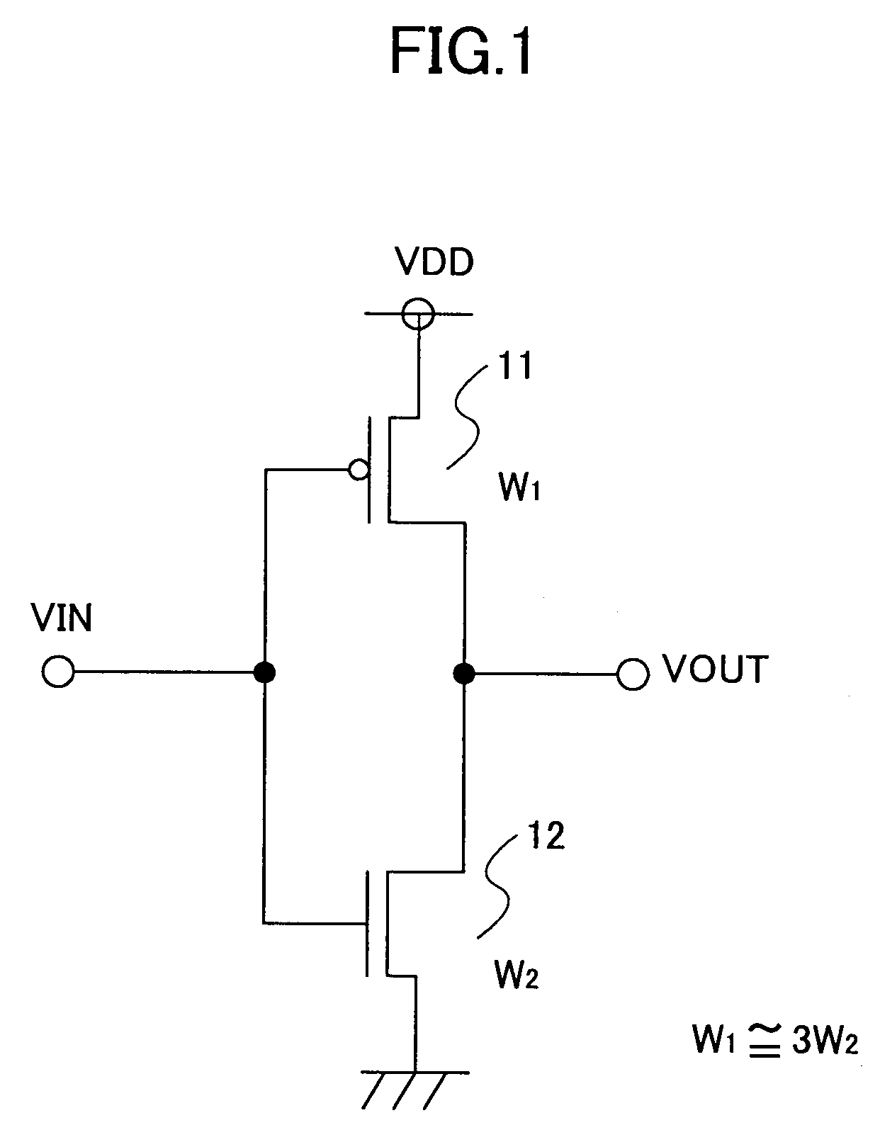
However, there arises various difficulties when using of such a conventional CMOS device construction due to the fact that the area of the channel region of the p-channel MOS transistor becomes larger than the area of the channel region of the n-channel MOS transistor, in that it becomes necessary to array the devices of different sizes at the time of designing highly miniaturized high-speed integrated circuits.
Further, there arises a problem of increased parasitic capacitance in the p-channel MOS transistor having a large area, while such an increase of parasitic capacitance causes the problem of degradation of operational speed and increase of power consumption.
Further, it should be noted that such a CMOS circuit shows non-linear operational characteristics due to the asymmetry of characteristics between the p-channel MOS transistor and the n-channel MOS transistor, while the existence of such an asymmetric characteristics imposes a limitation when the CMOS circuit is to be applied to analog circuits, and the like, in which a linear operation is required.
Thus, there has been a difficulty in handling a wafer particularly in the case the diameter of the wafer is increased.

Method used


Image

  • Complementary MIS device
  • Complementary MIS device
  • Complementary MIS device

Examples


first embodiment

[0056]FIGS. 6 and 7 show the construction of a CMOS device 30 according to a first embodiment of the present invention, wherein it should be noted that FIG. 7 is a diagram showing a part of FIG. 6.

[0057]Referring to FIGS. 6 and 7, the CMOS device 30 is constructed on a Si substrate having a (100) principal surface on which a region A and a region B are formed with a separation from each other by a device isolation region 31C. As represented in FIG. 7, the region A is formed with a projection 31A having a width W1A and a height HA, while the region B is formed with a projection 31B having a width W1B and a height HB at both lateral sidewalls. As can be seen from FIG. 7, the top surfaces of the projections 31A and 31B are defined by the (100) surface, while the sidewall surfaces thereof are defined by the (110) surface.

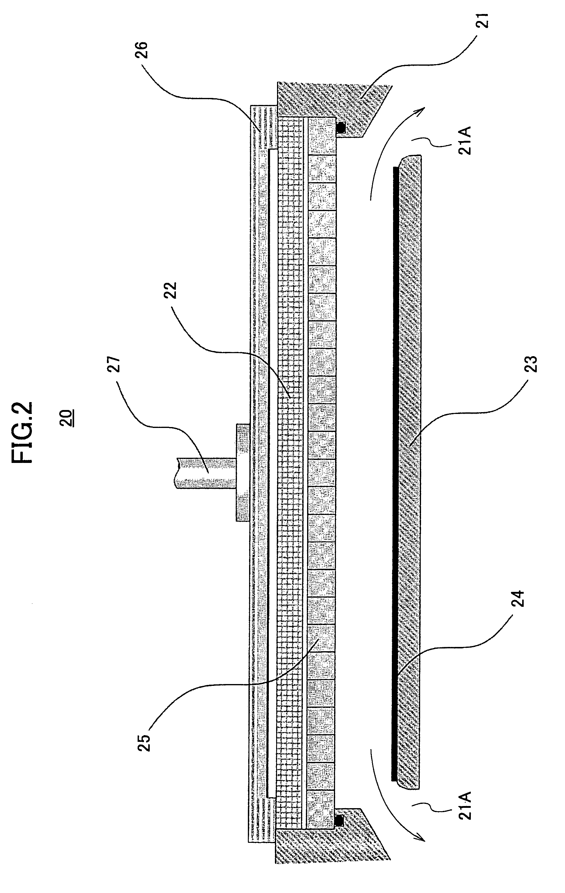
[0058]On the Si substrate 31 of FIG. 7, a silicon oxide film is formed uniformly by using the substrate processing apparatus 20 explained with reference to FIG. 2, and ...

second embodiment

[0067]FIG. 8 shows the construction of a CMOS device 40 according to a second embodiment of the present invention.

[0068]Referring to FIG. 8, the CMOS device 40 is formed on a Si substrate 41 having a (111) surface or a (110) surface as the principal surface and includes an n-channel MOS transistor 40A having a gate electrode 42A extending on the Si substrate 41 in a first orientation and a p-channel MOS transistor 40B having a gate electrode 42B extending on the Si substrate in a second, different orientation. At both lateral sides of the gate electrode 42A, there are formed n-type diffusion regions 43A and 44A. Similarly, p-type diffusion regions 43B and 44B are formed at both lateral sides of the gate electrode 42B.

[0069]Thereby, it should be noted that there is formed a CMOS circuit by connecting the diffusion region 44A and the diffusion region 43B and by connecting the gate electrodes 42A and 42B.

[0070]In the CMOS device of such a construction, it should be noted that the curre...

third embodiment

[0072]FIG. 9 shows the construction of a three-input NAND circuit that uses the CMOS circuit of any of the foregoing embodiments.

[0073]Referring to FIG. 9, the three-input NAND circuit includes n-channel MOS transistors Tr1–Tr3 connected in series between an output line connected to an output terminal and a ground line, while there are connected p-channel MOS transistors Tr4–Tr6 in parallel between an output line VOUT and a supply voltage source VDD. Thereby, an input logic signal A is supplied to respective gates of the MOS transistors Tr1 and Tr4, while another input logic signal B is supplied to respective gates of the MOS transistors Tr2 and Tr5. Further, an input logic signal C is supplied to respective gates of the MOS transistors Tr3 and Tr6.

[0074]In FIG. 9, it should be noted that the numerals attached to the transistors indicate the relative device area of the respective transistors. Thus, in the case the entire transistors are formed on the (100) surface of silicon, it wil...


PUM


Abstract

A CMOS device includes a p-channel MOS transistor and an n-channel MOS transistor having a structure formed on a (100) surface of a silicon substrate and having a different crystal surface, a high-quality gate insulation film formed on such a structure by a microwave plasma process, and a gate electrode formed thereon, wherein the size and the shape of the foregoing structure is set such that the carrier mobility is balanced between the p-channel MOS transistor and the n-channel MOS transistor.

Description

TECHNICAL FIELD[0001]The present invention generally relates to semiconductor devices and more particularly to a complementary MIS device in which the carrier mobility is balanced between a p-channel MOS transistor and an n-channel MOS transistor.BACKGROUND ART[0002]A CMOS circuit is a fundamental electronic circuit that includes a p-channel MOS transistor and an n-channel MOS transistor. Thus, CMOS devices constituting such a CMOS circuit are used extensively in various electronic apparatuses.[0003]Conventionally, a CMOS device has been formed on a (100) surface of a Si substrate, on which it is possible to form a high-quality thermal oxide film.[0004]On the (100) surface of a Si substrate, on the other hand, there appears a significant difference in the effective mass and lattice scattering probability between the electrons and holes, and because of this, the electron mobility takes a value twice or three times as large as that of the hole mobility.[0005]FIG. 1 shows the circuit o...

Claims


Application Information

Patent Timeline
IPC IPC(8): H01L29/76H01L21/8238H01L27/092H01L29/04H01L29/786
CPCH01L21/823807H01L21/823821H01L27/092H01L29/045H01L27/0922H01L29/7851H01L29/66795H01L21/8238
Inventor OHMIKOTANI, KOJISUGAWA, SHIGETOSHI
Owner TOHOKU UNIV
Learn More