
Multiple gate semiconductor device and method for forming same

a semiconductor device and multi-gate technology, applied in the field of integrated circuits, can solve the problems of reducing the saturation current of the semiconductor device, affecting the performance of the finfet device manufactured in such a fashion, and affecting the performance of the finfet device manufactured in the same processing technology, so as to achieve the effect of improving performan

Active Publication Date: 2007-04-10
INTERUNIVERSITAIR MICRO ELECTRONICS CENT (IMEC VZW)
View PDF16 Cites 308 Cited by
  • Summary
  • Abstract
  • Description
  • Claims
  • Application Information

AI Technical Summary

Benefits of technology

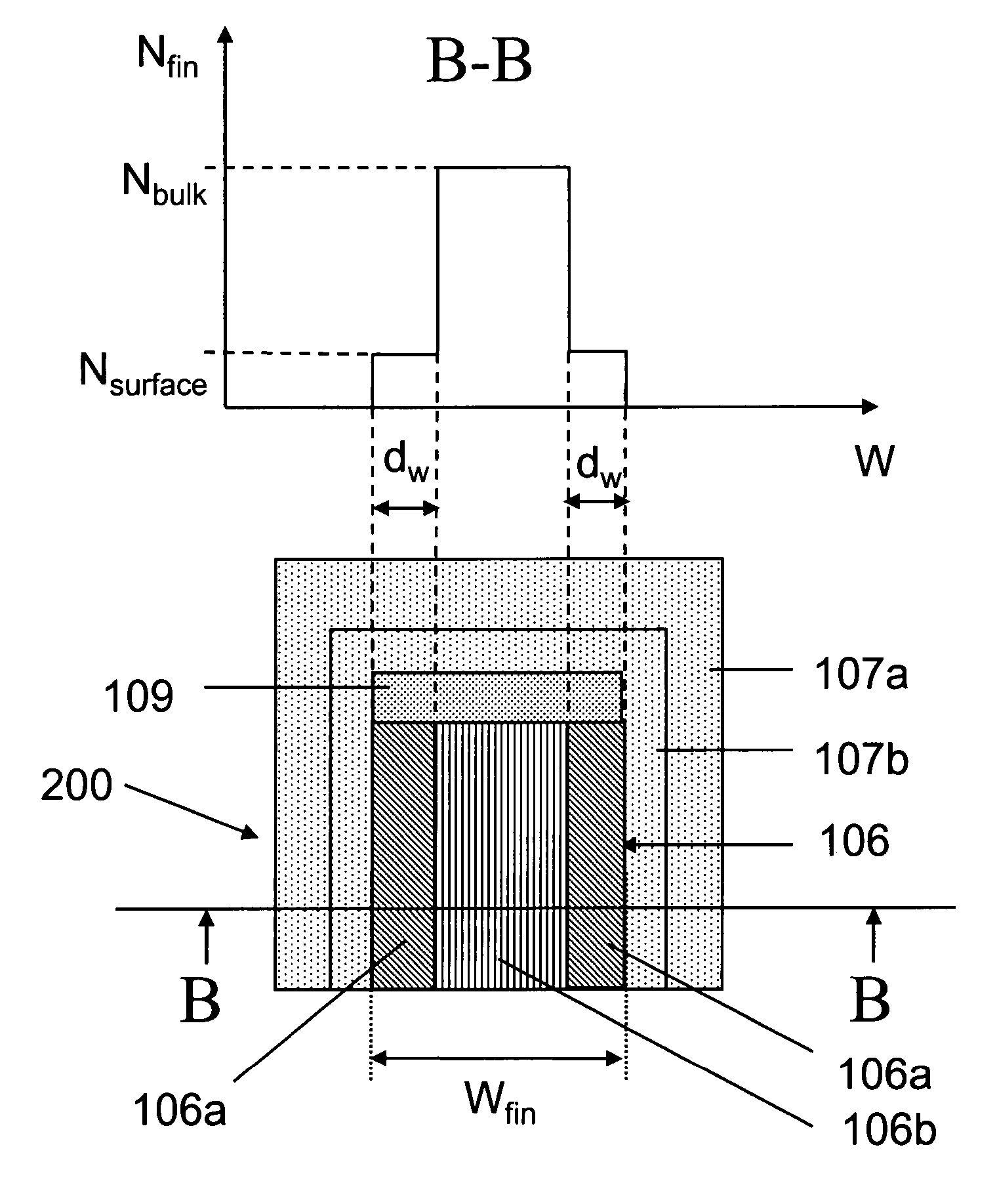
The invention addresses performance issues in current FinFET approaches by introducing a multi-gate semiconductor device with a retrograde doping profile. The device has a source, drain, and a semiconductor body with a first region having a first dopant level and a second region with a second dopant level lower than the first level. The second region is located between the gate electrode and the first region. The method for manufacturing the device includes forming a layer with a lower dopant level at the exposed surfaces of the fin. The device has improved performance without degrading other device parameters such as sub-threshold slope, saturation current, leakage current, and threshold voltage roll-off.

Problems solved by technology

While is possible for a FinFET be manufactured in a near-planar fashion, such that the manufacturing is compatible with traditional CMOS processing technologies, the performance of FinFET devices manufactured in such a fashion is typically inferior to traditional planar CMOS transistors manufactured with the same processing technology.
Although this approach yields a low sub-threshold slope and a controllable threshold voltage, during operation, when inversion occurs near the surface of the fin, the carrier mobility is degraded due to ionized impurity scattering.
This results in a lower saturation current, which slows down the device and reduces its performance.
Further, in such an approach, threshold voltage roll-off will be more pronounced, as the highly doped fin will typically not become fully depleted during operation.
This approach is cumbersome, as only a limited selection of materials is available, thereby still requiring additional efforts to tune the work function of these materials to the desired value.
The introduction of such materials increases the manufacturing process complexity as additional process steps may be employed.
Still further, the low doping concentration of the fin results in a higher sub-threshold slope and, consequently, in increased leakage current and increased power consumption as is described in “A Comprehensive Model Analytical Sub-threshold Swing (S) Model for Double-gate MOSFETs” by Qiang Chen et al, in IEEE Transactions on Electronic Devices, Vol. 49, No. 6, Jun. 2002, p.

Method used


Image

  • Multiple gate semiconductor device and method for forming same
  • Multiple gate semiconductor device and method for forming same
  • Multiple gate semiconductor device and method for forming same

Examples


Embodiment Construction

[0024]While embodiments of multiple gate semiconductor devices are generally discussed herein with respect to Fin Field Effect Transistors (FinFETs), it will be appreciated that the invention is not limited in this respect and that embodiments of the invention may be implemented in any number of types of device. For example, in his article “Beyond the Conventional Transistor”, published in IBM Journal of Research & Development, Vol. 46, No. 23 2002, which in incorporated by reference herein in it entirety, H. S. Wong discloses various types of multi-gate devices. In FIG. 14, 15 and 17 of this paper, alternative orientations of double and triple gate devices are depicted with the corresponding process sequences being detailed on pages 146–152. Such device configurations may be employed with embodiments of the invention.

1. Current FinFET Device

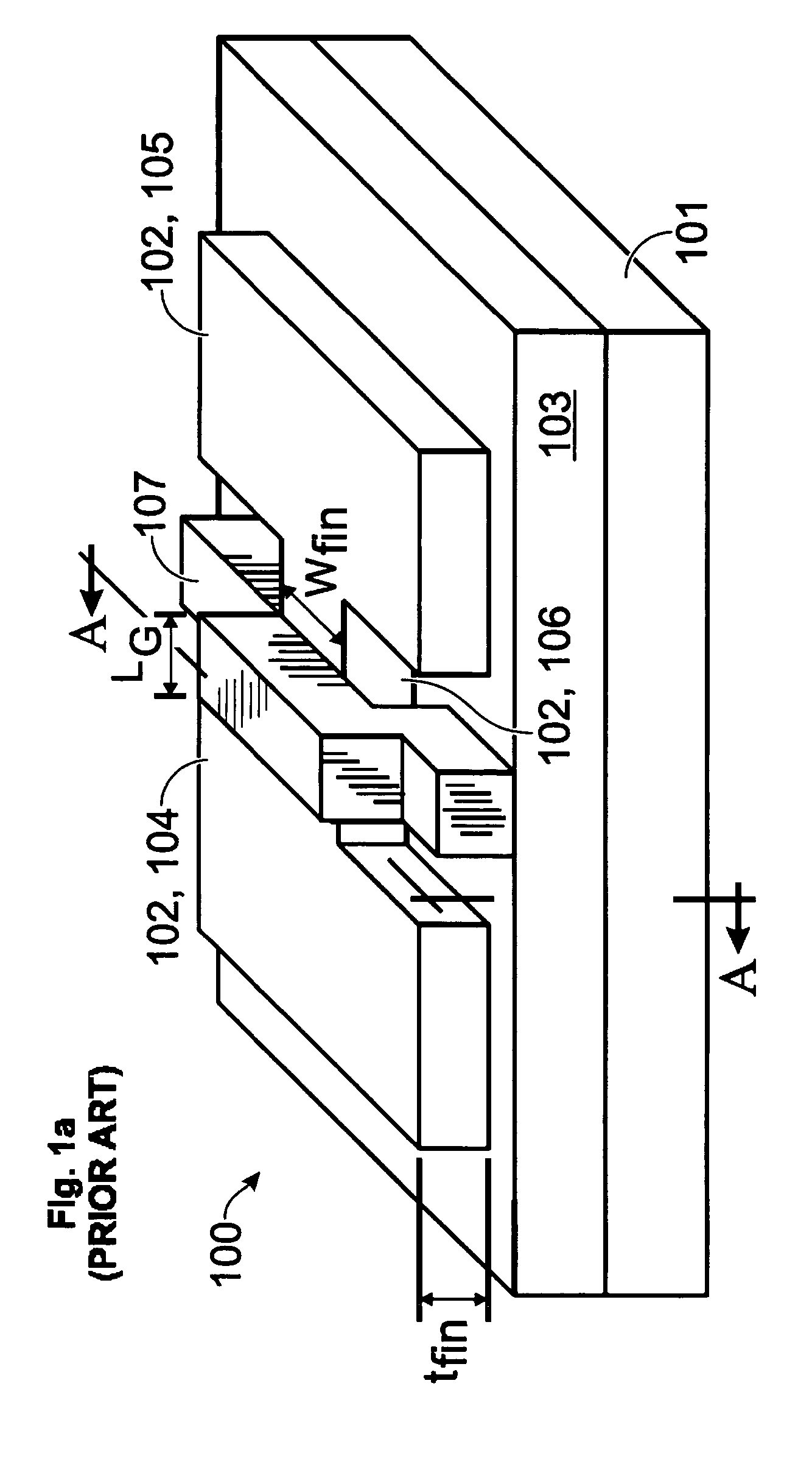
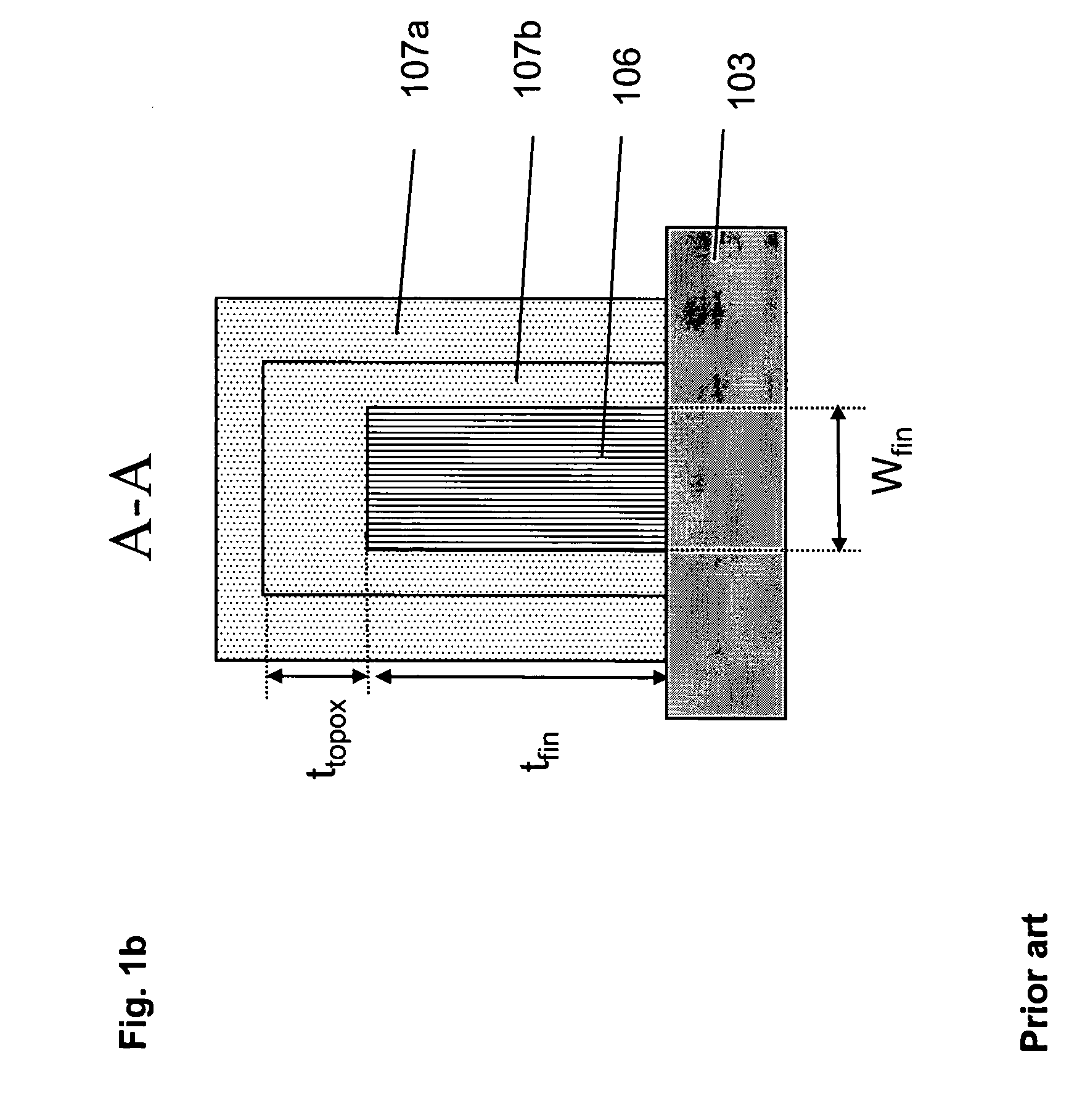
[0025]FIG. 1a is a drawing of a prior art FinFET device 100. The FinFET device 100 includes a semiconductor layer 102 disposed on a substrate 1...


PUM


Abstract

A multiple gate semiconductor device. The device includes at least two gates. The dopant distribution in the semiconductor body of the device varies from a low value near the surface of the body towards a higher value inside the body of the device.

Description

CROSS REFERENCE TO RELATED APPLICATIONS[0001]This application claims the benefit under 35 U.S.C. § 119(e) of U.S. Provisional Patent Application No. 60 / 488,328, filed on Jul. 18, 2003 and under 35 U.S.C. § 119(a) of European patent application EP 03447238.1, filed on Sep. 25, 2003. U.S. Provisional Patent Application No. 60 / 488,328 and European patent application EP 03447238.1 are herein incorporated by reference in their entirety.BACKGROUND[0002]1. Field of the Invention[0003]This invention is related to integrated circuits and methods for manufacturing such integrated circuits. More particularly, the present invention relates to semiconductor devices with multiple gates and non-uniform doping profiles in the channel region of those devices.[0004]2. Description of Related Art[0005]Current semiconductor chips feature technology with circuit feature sizes in the range of 130 nanometers, with components manufactured with technologies having 90 nanometer feature sizes just beginning to...

Claims


Application Information

Patent Timeline
Patent Type & Authority Patents(United States)
IPC IPC(8): H01L29/78H01L21/336H01L29/10H01L29/786
CPCH01L29/1041H01L29/105H01L29/66795H01L29/785
Inventor DIXIT, ABHISEKDE MEYER, KRISTIN
Owner INTERUNIVERSITAIR MICRO ELECTRONICS CENT (IMEC VZW)
Learn More