High-speed differential logic multiplexer

a digital multiplexer and high-speed technology, applied in logic circuits, electronic switching, pulse techniques, etc., can solve the problems of poor load drive capability of current mode logic, poor speed vs. fan-in (i.e., the number of inputs in a gate), and increase the scale of input devices, so as to reduce the rc time constant

Active Publication Date: 2007-04-03
ANALOG DEVICES INC
View PDF4 Cites 6 Cited by
  • Summary
  • Abstract
  • Description
  • Claims
  • Application Information

AI Technical Summary

Problems solved by technology

But the loads for differential current mode logic circuits are simply resistors, and thus, current mode logic suffers from poor load drive capability and poor speed vs. fan-in (i.e., number of inputs in a gate) trade off.
And as data speeds approach and surpass the 1 GHz threshold, circuit reactances create various problems which are not so significant at lower data speeds.
And increasing the scale of the input devices provides no speed improvement because the circuit is limited by self-loading.

Method used


Image

  • High-speed differential logic multiplexer
  • High-speed differential logic multiplexer
  • High-speed differential logic multiplexer

Examples


Embodiment Construction

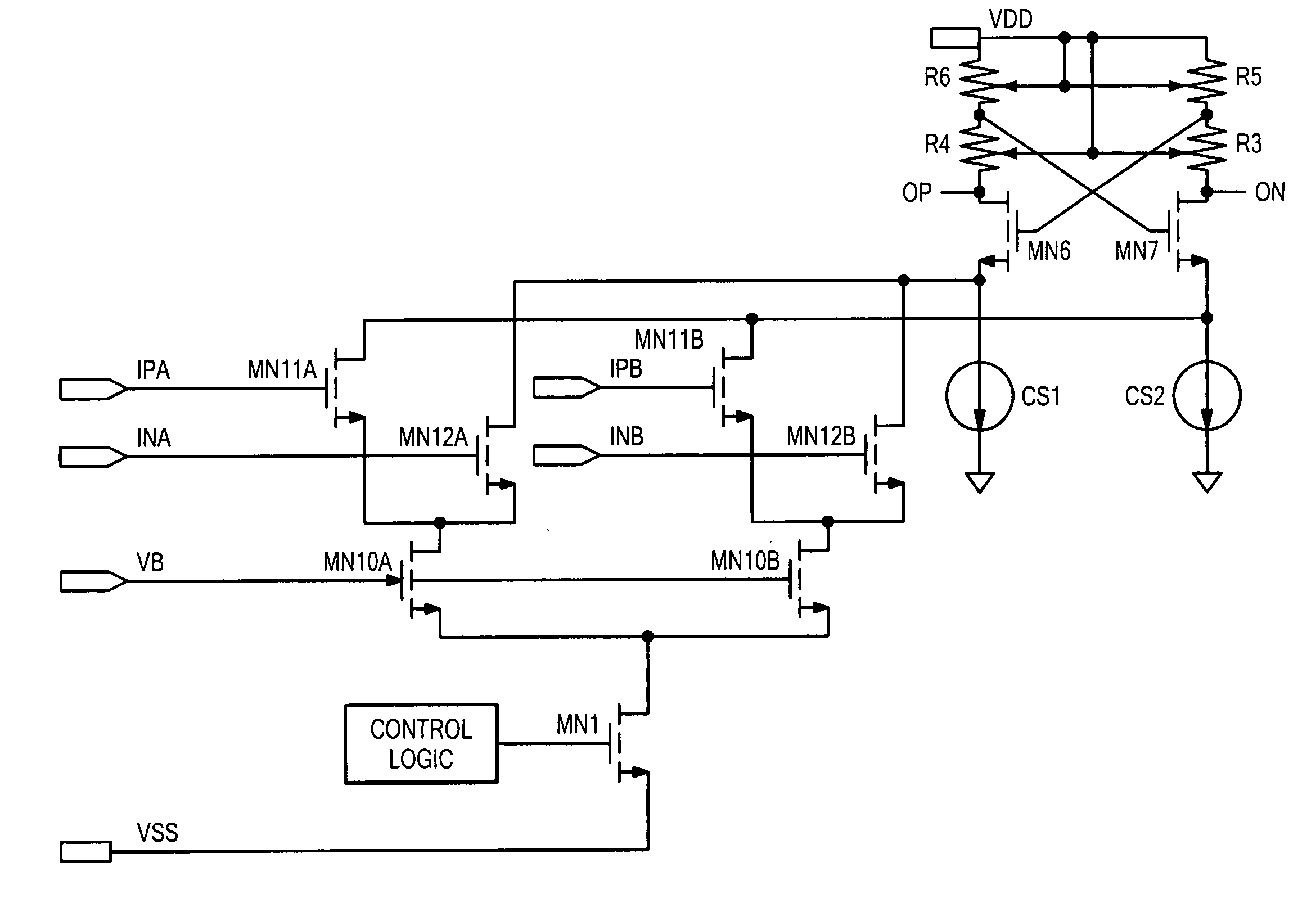
[0014]Various embodiments of the present invention are directed to techniques for using an active load circuit to reduce the RC time constant at the output terminals of a high speed digital multiplexer (common terminals which are also the active load circuit inputs) such as is used in a crosspoint switch. Such an approach allows for a current mode logic implementation of such high fan-in circuits with reduced delay and low-complexity overhead. The multiplexer can be implemented as an array of simple input stages and a low-input-impedance load. This facilitates implementation of high-speed crosspoint switches.

[0015]FIG. 3 shows the switching structure for a multiplexer according to one embodiment of the present invention. One data path enters the figure on the upper left side as lines IPA and INA to the gates of differential switch pair MN11A and MN12A, and output via the drains of MN11A and MN12A. Another data path enters on lines IPB and HNB to the gates of differential switch pair...


PUM


Abstract

A circuit for a high speed digital multiplexer has an active load circuit connected to an output of the digital multiplexer. The active load circuit loads the multiplexer output with a transimpedance stage with low input resistance to reduce the RC time constant at the multiplexer output. The active load circuit may be based on two active devices connected to the multiplexer output so as to form a differential cascode circuit.

Description

FIELD OF THE INVENTION[0001]The invention generally relates to data switching circuits, and more specifically to an active load circuit for a high speed digital multiplexer.BACKGROUND ART[0002]Complex digital data circuits use various architectures to distribute data signals between multiple locations. A digital crosspoint switch can selectably connect data signals between multiple inputs and multiple outputs. One way to implement a crosspoint switch is as an array of multiplexer stages. For example, a 32×32 crosspoint switch can be implemented as an array of thirty-two 32:1 multiplexers which share a 32-input bus.[0003]FIG. 1 shows the functional block architecture of a typical crosspoint switch. The left edge of the figure shows inputs 0–39 and the bottom edge shows outputs 0–35. Any input can be connected to any number of outputs. Each of the smaller dashed line boxes along the left side of FIG. 1 represents a two-stage input buffer. The larger dashed line boxes in the center of ...

Claims


Application Information

Patent Timeline
Patent Type & Authority Patents(United States)
IPC IPC(8): H03K19/094H03K17/00
CPCH03K3/35613H03K17/005H03K17/693
Inventor TAM, KIMO Y. F.
Owner ANALOG DEVICES INC
Why Eureka
Try Eureka