Basic cell, edge cell, wiring shape, wiring method, and shield wiring structure
a shielding and wire technology, applied in the field of shield wiring technique, can solve the problems of no free space left, man-hour wiring, etc., and achieve the effects of increasing processing difficulty, low regularity, and double the processing time required
- Summary
- Abstract
- Description
- Claims
- Application Information
AI Technical Summary
Benefits of technology
Problems solved by technology
Method used
Image
Examples
embodiment 1
[0060
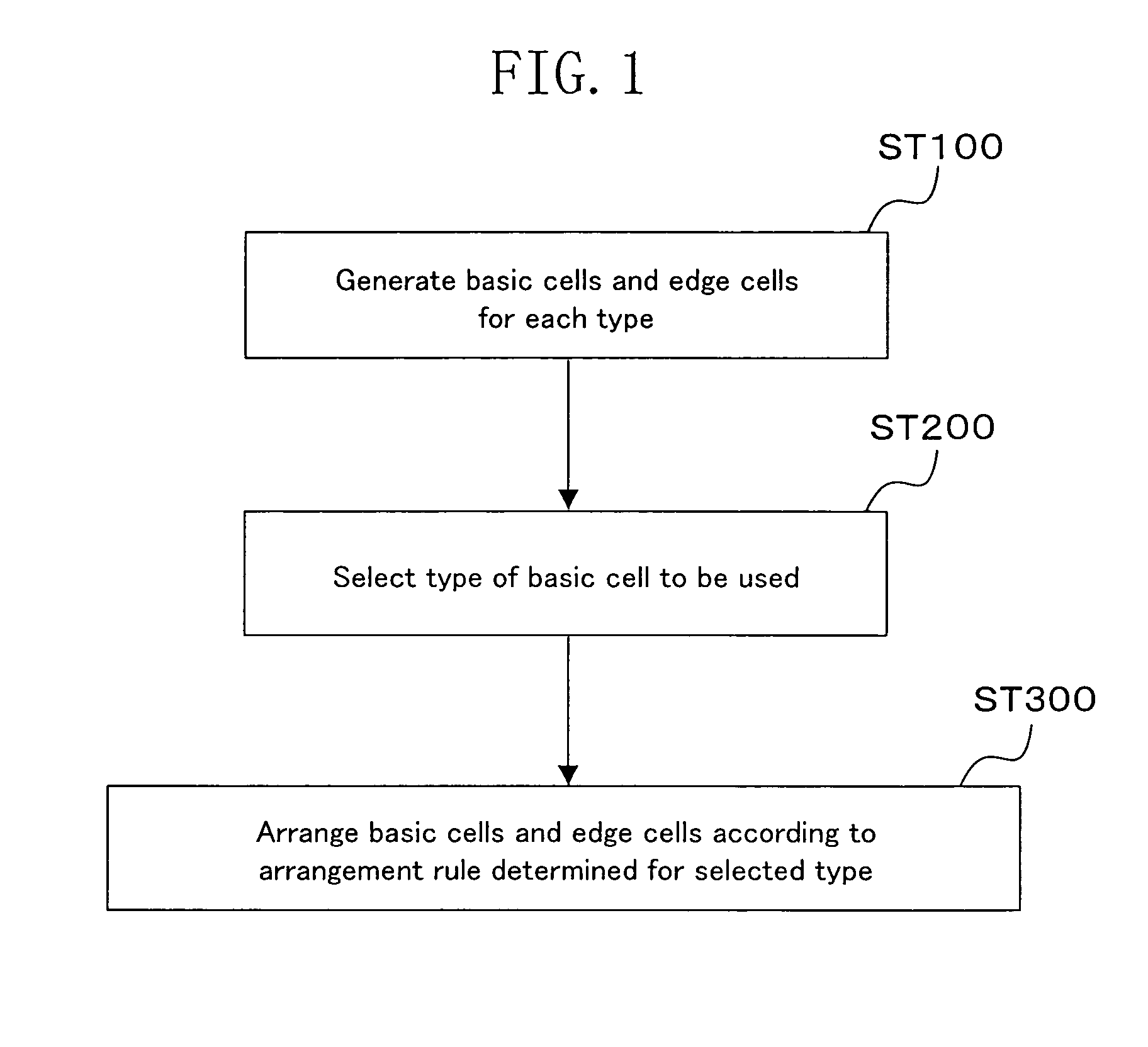
[0061]FIG. 1 shows a general procedure of a shielding line wiring method according to embodiment 1. A shielding line is provided in the uppermost wiring layer to hide a mask pattern, whereby reading of the mask pattern and circuit analysis with a probe on wires, which are performed for the purpose of copying and tampering of a semiconductor chip, are prevented. In embodiment 1, a plurality of wiring patterns (basic cells) each having a small area are prepared, and selection and arrangement of the wiring patterns are performed on a random basis. It should be noted that, as a matter of course, adjoining basic cells may have the same pattern. With this feature, shielding wires of low regularity, which is different from a simple array configuration, can be generated. Generation of such shield wiring is described below in detail.
100)>
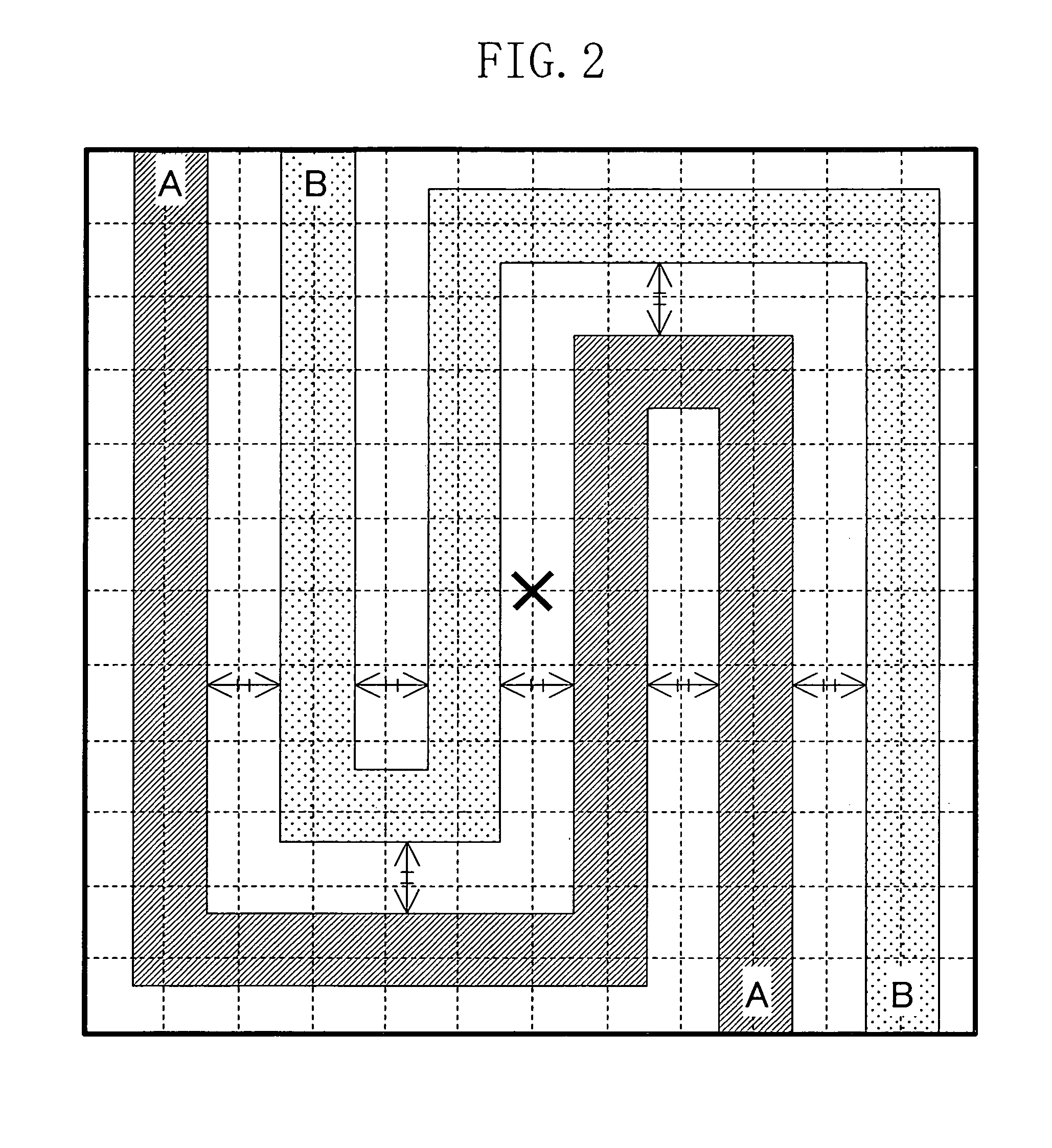
[0062]First, a design rule of a wiring pattern (basic cell) which is a basic unit of shield wiring is described. FIG. 2 shows an example of a basic cel...
embodiment 2
[0109
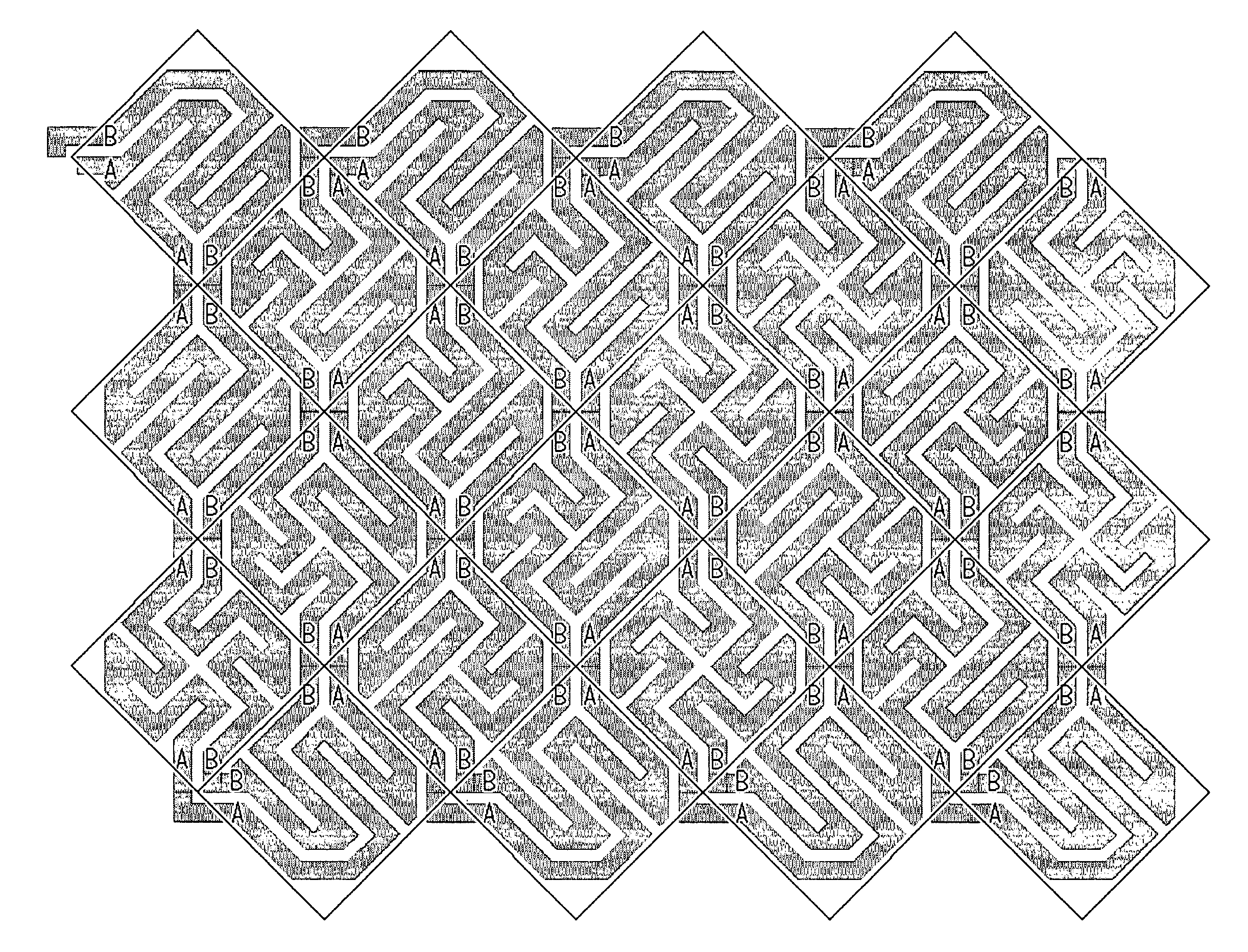
[0110]The general procedure of the shielding line arrangement method of embodiment 2 is the same as that illustrated in FIG. 1. In embodiment 2, basic cells are arranged to form a plurality of constantly-parallel routes, and edge cells are arranged such that the same route is not adjacently provided (i.e., a route does not adjoin itself). Even if circuit analysis is committed with a probe against a circuit line in a shielding line removed region, the above structure of embodiment 2 doubles the processing time required for analysis in a region including two or more routes of shielding lines. Accordingly, the processing difficulty increases. This feature is specifically described below.
100)>
[0111]First, a design rule of a basic cell which is a basic unit of the shielding line is described. Herein, the following design rule is provided for obtaining uniform wiring density:[0112]External boundary of a basic cell is rectangular;[0113]In the uppermost wiring layer, wires extend strai...
embodiment 3
[0129
[0130]The structure of a basic cell according to embodiment 3 is shown in FIG. 30. In this basic cell, a 45°-route of the common 45°-wiring arrangement type basic cell illustrated in embodiments 1 and 2 is realized by a stepped route of 90°, whereby the difficulty level of treatment and processing of edge portions for 45° is lowered. In this basic cell, a stepped portion appears to be smooth like a 45°-wire. Further, due to the stepped shape, the exposed area of the underlying layer is small as compared with a common 45°-route. Although in FIG. 30 the entirety of the 45°-routes is realized by stepped 90°-routes, only a part of the 45°-routes may be realized by a stepped 90°-route. The basic cells illustrated in FIG. 30 are placed all over the shield region as in embodiments 1 and 2, whereby shielding lines are realized.
PUM
 Abstract
Description
Claims
Application Information
 - R&D
- Intellectual Property
- Life Sciences
- Materials
- Tech Scout
- Unparalleled Data Quality
- Higher Quality Content
- 60% Fewer Hallucinations
Browse by: Latest US Patents, China's latest patents, Technical Efficacy Thesaurus, Application Domain, Technology Topic, Popular Technical Reports.
© 2025 PatSnap. All rights reserved.Legal|Privacy policy|Modern Slavery Act Transparency Statement|Sitemap|About US| Contact US: help@patsnap.com


