
Exposure apparatus and device manufacturing method

a technology of exposure apparatus and manufacturing method, which is applied in the direction of instruments, printers, therapy, etc., can solve the problems of serious decrease in device production yield and degradation of device reliability

Inactive Publication Date: 2007-03-20
CANON KK
View PDF10 Cites 12 Cited by
  • Summary
  • Abstract
  • Description
  • Claims
  • Application Information

AI Technical Summary

Benefits of technology

The present invention provides an improved exposure apparatus for manufacturing semiconductor devices. The apparatus includes an optical system, an exposure chamber, and a load-lock chamber. The load-lock chamber is designed to create a vacuum atmosphere around the substrate to prevent contamination during the exposure process. The load-lock chamber is heated to a higher temperature than the exposure chamber to prevent water vapor from condensing during the exhaust of gas. The load-lock chamber is designed to start the conversion of the ambient space around the substrate when the gas inside it reaches a predetermined temperature or when a certain time period has passed. The apparatus may also include a heat insulating material or structure between the load-lock chamber and the exposure chamber, gas supply means with temperature adjusting means, and a deformable member for relative displacement. The invention aims to improve the efficiency and accuracy of the exposure process.

Problems solved by technology

This causes a serious decrease of yield of device production and degradation of device reliability.
Furthermore, the above-described phenomenon of water vapor condensation causes serious problems even without the presence of particles inside the load-lock chamber that function as nuclei, the problems being that various ions inside the gas function as a condensation nucleus (heterogeneous nucleation condensation), or that water vapor is coagulated and grows largely (homogeneous nuleation).
Thus, the presence of water vapor inside the load-lock chamber, itself, is the source of the problem.

Method used


Image

  • Exposure apparatus and device manufacturing method
  • Exposure apparatus and device manufacturing method
  • Exposure apparatus and device manufacturing method

Examples


embodiment 1

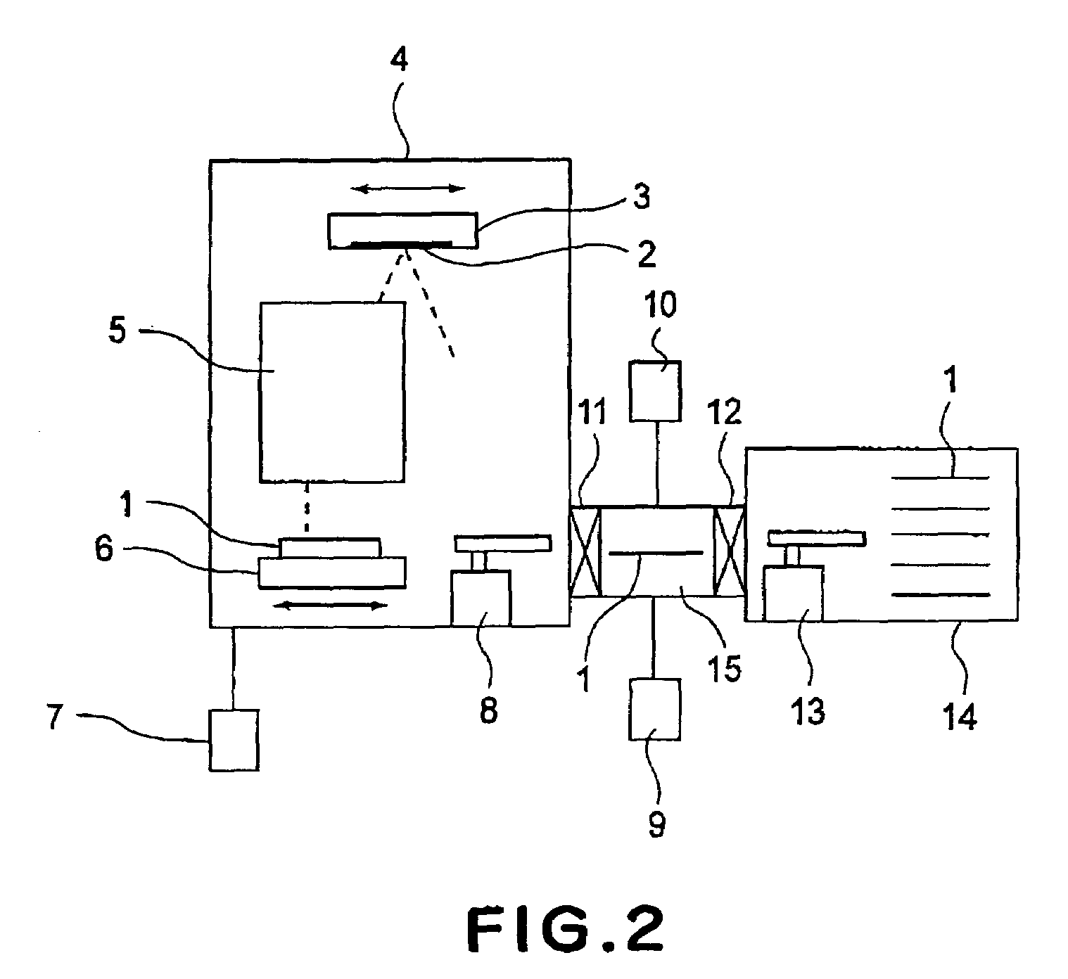
[0048]First of all, a projection exposure apparatus to which the present invention is applied will be explained, with reference to an EUV exposure apparatus shown in FIG. 2 of the drawings.

[0049]In FIG. 2, denoted at 1 is a wafer, and denoted at 2 is a reflection type mask having an electronic circuit pattern formed thereon. Denoted at 3 is a mask stage for holding a reflection type mask thereon and for coarsely and finely moving the same in a scan direction, and denoted at 5 is an optical system for directing reflection light from the mask to a wafer 1 for projection exposure thereof. Denoted at 6 is a wafer stage for holding a wafer thereon and for coarsely and finely moving the same in six-axis directions. The position of the wafer stage with respect to the X- and Y-axis directions is continuously monitored by means of laser interferometers (not shown). Normally, the scan motion of the mask stage 3 and the wafer stage 6 is synchronously controlled to assure that, when the reducti...

embodiment 2

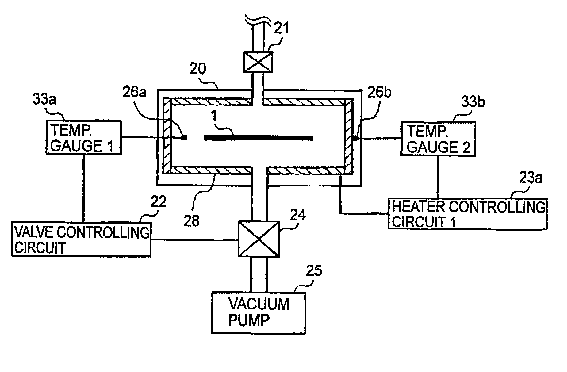
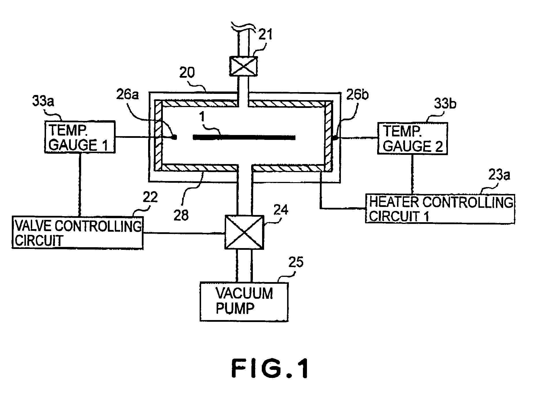
[0079]A second embodiment of the present invention pays a specific note to the throughput. As an important feature, in relation to the supply of a vent gas into the chamber, a gas heating mechanism is provided separately from the load-lock chamber wall heating means, thereby to assure that a gas having a temperature raised beforehand up to a predetermined temperature is supplied into the chamber. This enables initiation of vacuum evacuation just after the wafer exchange.

[0080]Referring to FIG. 16, this embodiment will be described in detail. This embodiment differs from the first embodiment in that there is a heat exchanger 35 at an upstream position of a vent valve 21. The heat exchanger comprises a heater and a large number of fins connected thereto. Disposed downstream of this heat exchanger is a sensor 26c for measuring the gas temperature, the sensor being provided in a pipe. In association with a temperature gauge 3 (33c), the temperature of the heated gas can be measured. Den...

embodiment 3

[0084]Next, referring to FIGS. 21 and 22, an embodiment of a device manufacturing method, which uses an exposure apparatus described above, will be explained.

[0085]FIG. 21 is a flow chart for explaining the procedure of manufacturing various microdevices, such as semiconductor chips (e.g., ICs or LSIs), liquid crystal panels, or CCDs, for example. Step 1 is a design process for designing a circuit of a semiconductor device. Step 2 is a process for making a mask on the basis of the circuit pattern design. Step 3 is a process for preparing a wafer by using a material such as silicon. Step 4 is a wafer process, which is called a pre-process, wherein, by using the thus prepared mask and wafer, a circuit is formed on the wafer in practice, in accordance with lithography. Step 5, subsequent to this, is an assembling step, which is called a post-process, wherein the wafer having been processed at step 5 is formed into semiconductor chips. This step includes an assembling (dicing and bondin...


PUM

PropertyMeasurementUnit
temperatureaaaaaaaaaa

Abstract

An exposure apparatus for exposing a substrate. The apparatus includes an optical system being set at a reference temperature, for directing light to the substrate, an exposure chamber for storing the optical system in a vacuum ambience, and a load-lock chamber, disposed adjacent to the exposure chamber, for converting an ambience of a space surrounding the substrate into a vacuum ambience. When the load-lock chamber converts the ambience of the space surrounding the substrate into a vacuum ambience, the temperature of the load-lock chamber is made higher than the reference temperature.

Description

FIELD OF THE INVENTION AND RELATED ART[0001]This invention relates generally to a semiconductor exposure apparatus. More particularly, the invention concerns an exposure apparatus having a load-lock chamber, which is provided in association with an apparatus for exposing a semiconductor substrate in a vacuum ambience.[0002]In relation to semiconductor devices, such as DRAMs or MPUs, for example, much research and many developments are currently being done to achieve devices having a linewidth of 0.11 μm or less in design rule. The exposure apparatuses to be used for this generation will be those using an electron beam (EB) or extreme ultraviolet light (EUV).[0003]In such EB or EUV exposure apparatuses, exposure in atmosphere is impracticable. The exposure has to be done in a vacuum and, hence, the wafer loading and unloading should be made by way of a load-lock chamber.[0004]Generally, the load-lock chamber functions so that it receives a wafer under atmospheric pressure and then, t...

Claims


Application Information

Patent Timeline
Patent Type & Authority Patents(United States)
IPC IPC(8): G03B27/42G03F7/20H01L21/00H01L21/027H01L21/677
CPCG03F7/70525G03F7/70808G03F7/70841G03F7/7085H01L21/67248G03F7/70916H01L21/67126H01L21/67201H01L21/67225G03F7/70858
Inventor YONEKAWA, MASAMI
Owner CANON KK
Learn More