[0013]The present invention provides localized contaminant
layer removal from a thin film surface, thereby enabling accurate and repeatable analysis of the thin film by a measurement tool. By using a concentrated energy beam to clean only the portion of the thin film to be measured by the measurement tool, the thin film analysis can be performed without the long heating and cooling times associated with conventional cleaning systems. Furthermore, the compact components used in an energy beam-based cleaning
system can be incorporated into the thin film measurement tool itself, thereby eliminating any delays related to transferring the
wafer to and from a stand-alone cleaning system. This integration also minimizes the total
footprint required for a thin film analysis system, and since the
wafer can be cleaned and analyzed in the same process chamber, redeposition of contaminants on the cleaned portion of the
wafer can be prevented. In order to improve the cleaning of the substrate, and avoid damaging the substrate, a substantially flat-top profile is used for the energy beam. This substantially flat-top profile may be provided as described herein.
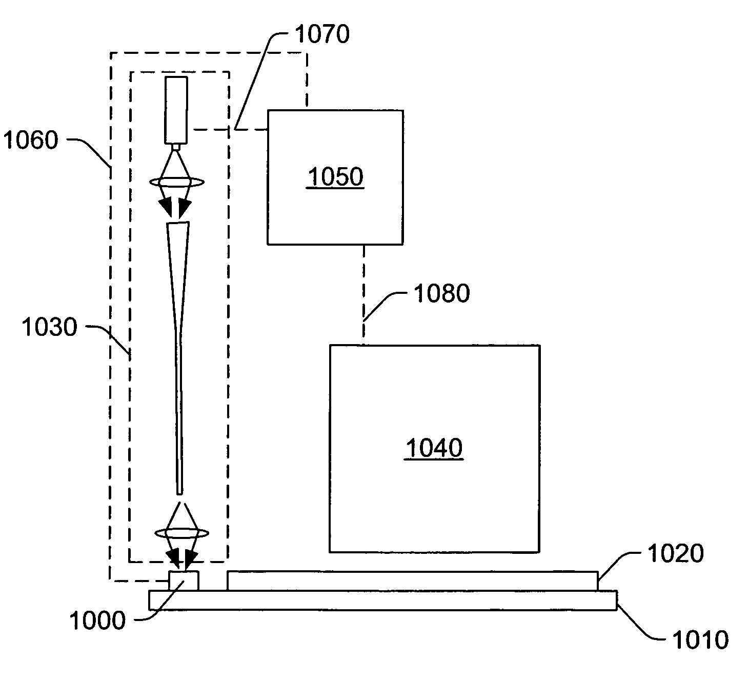
[0014]A thin film analysis system in accordance with an embodiment includes an energy
beam source, an analysis module, and a stage. The stage holds a
test sample (such as a wafer) that includes a thin film layer to be measured by the analysis module. The analysis module can include any thin film analysis system or systems, including a single-
wavelength ellipsometer (SWE, such as described in co-owned U.S. Pat. No. 6,734,968 to Wang et al.), a spectroscopic ellipsometer (SE, such as described in co-owned U.S. Pat. No. 5,608,526 to Piwonka-Corle et al.), a reflectometer (such as described in co-owned U.S. Pat. No. 5,747,813 to Norton et al.), a non-contact electrical measurement system (such as described in co-owned U.S. Pat. No. 5,485,091 to Verkuil), a GXR system (such as described in co-owned, U.S. Pat. No. 6,771,735, a contact-based electrical measurement system, an XRF system, and / or an EMP system. Each of these patents and
patent application are incorporated by reference as if fully set forth herein. More generally, this cleaning system can be used with any sort of inspection or
metrology system used in the production of
semiconductor devices. According to an embodiment, the energy
beam source is incorporated into a conventional thin film analysis tool, thereby minimizing the total
footprint of the thin film analysis system.
[0015]The energy beam source is configured to direct an energy beam at a contaminant layer on the surface of the thin film layer. The energy beam heats a portion of the contaminant layer until that portion of the contaminant layer is vaporized. This process can be aided by direct
photon excitation of the bonds between the contaminant layer and the thin film layer. The area of the thin film layer exposed by this cleaning operation can then be analyzed by the analysis module. The size of this analysis area required by the analysis module for performance of the thin film analysis can be used to determine the minimum required power and size of the energy beam. By minimizing the power and size of the energy beam, the risk of damage to the
test sample is small. This risk of damage can be further reduced by performing the cleaning and measuring operations at non-functional regions of the test sample. According to an embodiment, the energy beam source can include a
laser, such as a Q-switched
pulsed laser. In a different embodiment, the energy beam source can include a continuous (cw)
laser. According to another embodiment, the energy beam source can include a flashlamp with appropriate focusing
optics.
[0016]According to an embodiment, a probe beam generated by the analysis module (e.g., a low-power
laser beam, a
white light beam, a
corona discharge, an x-
ray beam, etc.) is directed at the same location on the test sample as the energy beam produced by the energy beam source. Alternatively, a physical probe structure (e.g., a four-point probe in a spreading resistance tool) can be aimed at the same location on the test sample as the energy beam produced by the energy beam source. Consequently, the test sample does not need to be moved between the cleaning and measurement operations, thereby maximizing analysis
throughput. Furthermore, because the measurement operation can be performed immediately after the cleaning operation, the chances of the cleaned portion of the thin film layer (i.e., the analysis area) being recontaminated before the measurement operation are minimized.
[0017]According to another embodiment, the probe beam (or probe structure) from the analysis module and the energy beam are directed at different locations on the test sample. The test sample (and / or the analysis module) is then repositioned after the cleaning operation to align the probe beam (or probe structure) with the analysis area of the thin film layer. This allows the focusing
optics or probe structure of the analysis module to be kept out of the vicinity of the portion of the contaminant layer being vaporized, thereby minimizing the risk of any contaminant redeposition on the measurement focusing
optics or probe structure. In each of the aforementioned embodiments, a substantially flat-top profile of the energy beam may be employed.
[0019]In contrast, the methods and systems described herein may efficiently couple an energy beam into the spatial mode spectrum of a
fiber to produce an energy beam that has a substantially flat-top profile, and in a more preferred embodiment, does so without having to resort to
static stress-induced
mode mixing (e.g., bending or twisting the
fiber).
