
Spin-on glass composition and method of forming silicon oxide layer in semiconductor manufacturing process using the same

a technology of spin-on glass and semiconductor manufacturing, which is applied in the direction of synthetic resin layered products, semiconductor/solid-state device details, liquid/solution decomposition chemical coatings, etc., can solve the problems of uneven surface of the first insulation layer, affecting the performance of the second metal layer, and increasing irregular topography of the top layer

Inactive Publication Date: 2007-02-20
SAMSUNG ELECTRONICS CO LTD
View PDF50 Cites 19 Cited by
  • Summary
  • Abstract
  • Description
  • Claims
  • Application Information

AI Technical Summary

Benefits of technology

[0013]Accordingly, it is a feature of an embodiment of the present invention to provide a spin-on glass composition that fills gaps between closely-spaced metal wirings of semiconductor devices having a high packing density and a large aspect ratio. It is also a feature of the present invention to provide a composition that fills gaps or smoothes surface discontinuities on a substrate without the need for mechanical planarization. It also is a feature of the invention to provide a spin-on glass composition that has substantially the same characteristics as an oxide layer of a semiconductor device formed by a chemical vapor deposition (CVD) method. It is another feature of the invention to provide a method of forming an oxide layer in a semiconductor manufacturing process using the above spin-on glass composition.

Problems solved by technology

In such a multilevel interconnection structure, the topography of the top layer usually is increasingly irregular and uneven as the number of layers increases.
At this time, the surface of the first insulation layer is uneven because the layers underlying the first insulation layer are uneven.
When the second metal layer is directly formed on the first insulation layer, the second metal layer may fracture due to protrusions or cracks in the underlying insulation layer.
In addition, there may be a decreased yield of the semiconductor device if the deposition state of the metal layer is poor.
However, depositing BPSG presents problems because it depends primarily on establishing special deposition parameters for the equipment utilized.
In addition, the gases used in the process are expensive and severely toxic.
Furthermore, as the packing density increases and the design rule gradually decreases for manufacturing VLSI having 256 megabits or more, using BPSG as the insulation layer to fill gaps between wirings lowers the yield due to the occurrence of voids and bridges.
In addition, an etch stop layer may possibly be damaged during its subsequent formation.
Thus, the prior art typically implements a reflowing process and an expensive CMP process to solve these problems.
In addition, because SOG is deposited by a spin coating method, the thickness of the thus formed silicon oxide layer is not sufficient.
This provides insufficient coverage for the conductive layers, such as gate electrodes and metal wirings.

Method used


Image

  • Spin-on glass composition and method of forming silicon oxide layer in semiconductor manufacturing process using the same
  • Spin-on glass composition and method of forming silicon oxide layer in semiconductor manufacturing process using the same
  • Spin-on glass composition and method of forming silicon oxide layer in semiconductor manufacturing process using the same

Examples


examples

[0050]Preparation of an SOG Composition

[0051]Perhydrpolyosilazane having a weight average molecular weight of 4,500–7,000 and a molecular weight dispersion of 3.0–4.0 was obtained by fractionating commercially available perhydropolysilazane. The fractionated perhydropolysilazane was dissolved in xylene to obtain an SOG composition having a perhydropolysilazane concentration of 22–25% by weight, based on the total weight of the composition. The contact angle of the SOG composition was 4° or less with respect to an underlying silicon nitride layer.

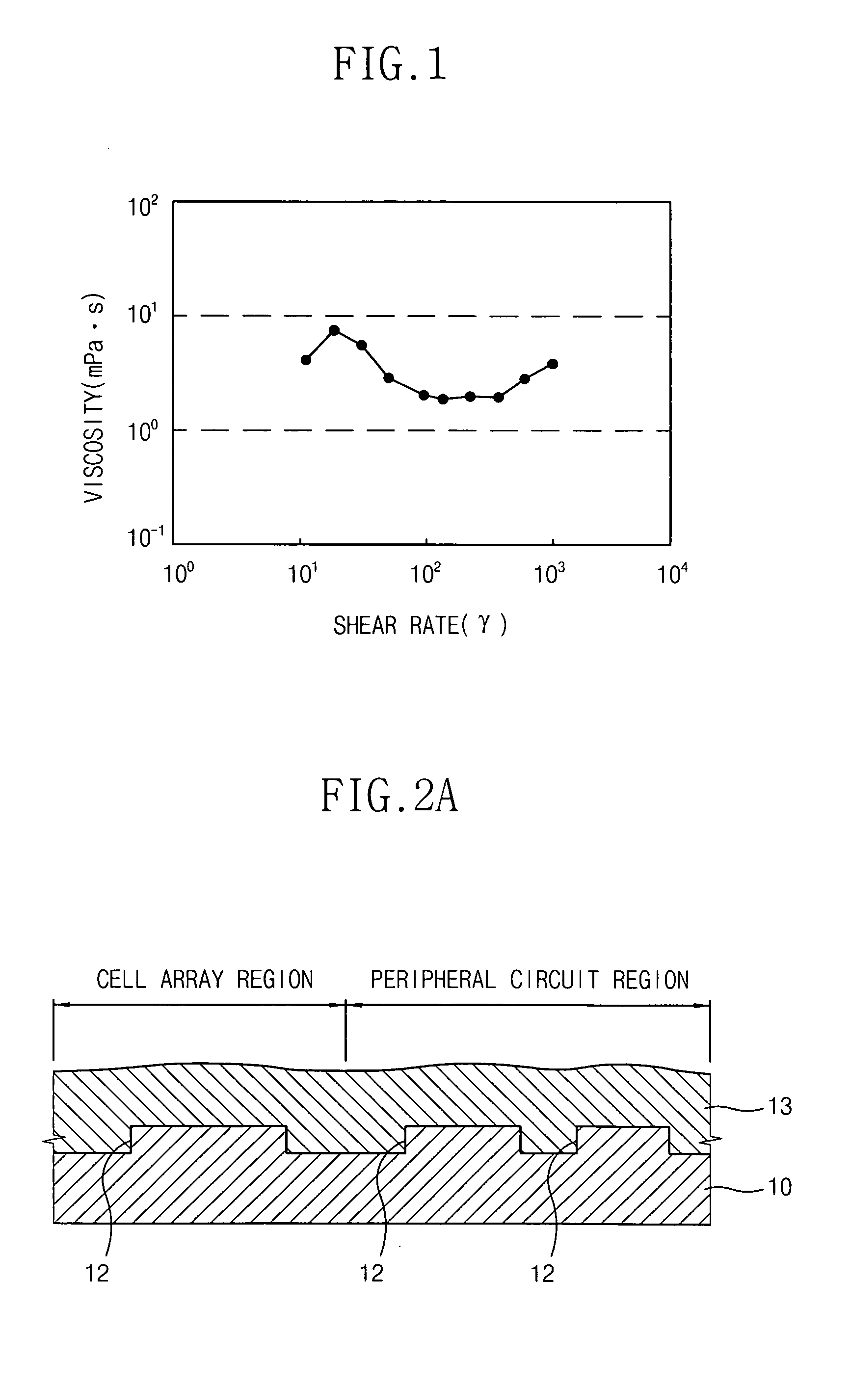
[0052]The viscosity of the SOG composition was detected according to the variation of its shear rate. The viscosity characteristic is illustrated in FIG. 1. FIG. 1 is a graph illustrating the viscosity change with respect to the shear rate change of the SOG solution. The ordinate represents the viscosity (mPa·s) and the abscissa represents the shear rate (1 / s). As can be seen in FIG. 1, the SOG solution preferably has a uniform viscosity wit...


PUM

PropertyMeasurementUnit
viscosityaaaaaaaaaa
contact angleaaaaaaaaaa
viscosityaaaaaaaaaa

Abstract

A spin-on glass (SOG) composition and a method of forming a silicon oxide layer utilizing the SOG composition are disclosed. The method includes coating on a semiconductor substrate having a surface discontinuity, an SOG composition containing perhydropolysilazane having a compound of the formula —(SiH2NH)n— wherein n represents a positive integer, a weight average molecular weight within the range of about 4,000 to 8,000, and a molecular weight dispersion within the range of about 3.0 to 4.0, to form a planar SOG layer. The SOG layer is converted to a silicon oxide layer with a planar surface by curing the SOG layer. Also disclosed is a semiconductor device made by the method.

Description

[0001]This application is a divisional application of U.S. Pat. application Ser. No. 09 / 686,624, filed Oct. 12, 2000, now U.S. Pat. No. 6,706,646, issued Mar. 16, 2004, which is incorporated by reference herein in its entirety.BACKGROUND OF THE INVENTION[0002]1. Field of the Invention[0003]The present invention relates to a spin-on glass (SOG) composition useful in forming a silicon oxide layer in a semiconductor manufacturing process, to a semiconductor device made thereby, and to a method of forming a silicon oxide layer using the same. More particularly, the present invention relates to a spin-on glass composition containing perhydropolysilazane, and its use in forming a silicon oxide layer in a semiconductor device.[0004]2. Description of the Related Art[0005]The design of semiconductor devices have recently made rapid progress. In particular, this progress has required semiconductor devices to function with high operating speed, and to have a large storage capacitance. In order...

Claims


Application Information

Patent Timeline
Patent Type & Authority Patents(United States)
IPC IPC(8): B32B27/06C08L83/04H01L21/31H01L21/768C08G77/62C09D183/00C09D183/16C23C18/12H01L21/3105H01L21/312H01L21/314H01L21/316H01L21/762H01L21/8234H01L23/522H01L27/088H10B12/00
CPCC08G77/62H01L21/823481C23C18/1212C23C18/122C23C18/1279C23C18/1283H01L21/02164H01L21/02222H01L21/02282H01L21/02337H01L21/31051H01L21/3125H01L21/316H01L21/31612H01L21/76229C09D183/16Y10T428/31663H01L21/02129H01L21/02126H01L21/02134
Inventor LEE, JUNG-HOCHOI, JUNG-SIKKIM, HONG-KILEE, DONG-JUNKANG, DAE-WONCHON, SANG-MUN
Owner SAMSUNG ELECTRONICS CO LTD
Learn More