Semiconductor device, method for manufacturing the same, circuit board, and electronic equipment
a technology of semiconductor devices and semiconductor components, applied in semiconductor devices, semiconductor/solid-state device details, electrical equipment, etc., can solve problems such as reliability affecting the bonding strength between upper and lower interposers, and achieve the effect of enhancing the strength of contact parts
- Summary
- Abstract
- Description
- Claims
- Application Information
AI Technical Summary
Benefits of technology
Problems solved by technology
Method used
Image
Examples
first embodiment
[0038
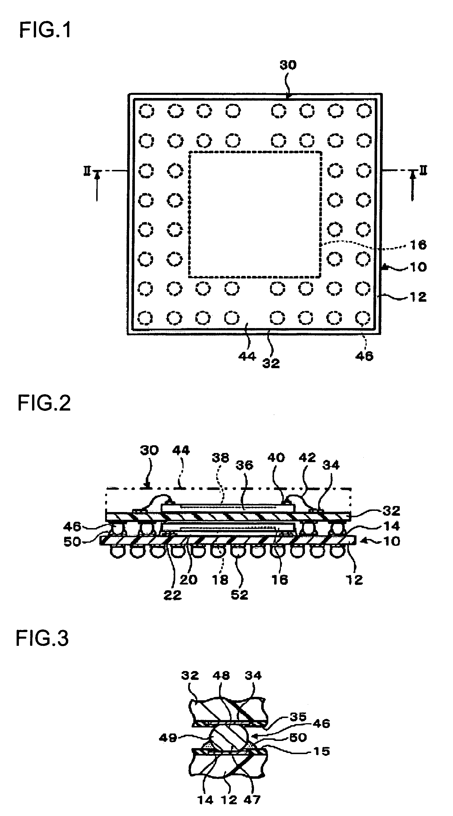
[0039]FIG. 1 is a plan view illustrating a semiconductor device according to a first embodiment of the present invention. FIG. 2 is a sectional view of the semiconductor device shown in FIG. 1 along the line II—II. FIG. 3 is a partial enlarged view of FIG. 2.
[0040]The semiconductor device includes a first package 10. The first package 10 has a first interposer 12. The first interposer 12 is a substrate, and may be a plate. The first interposer 12 may be rectangular. The first interposer 12 may be made of a resin such as polyimide resin, or of a mixed material of organic (e.g. resin) and inorganic materials. Alternatively, the first interposer 12 may be a metal or ceramic substrate. The first interposer 12 is provided with a first wiring pattern 14. The first wiring pattern 14 may include a wire for electrically coupling a plurality of points, and a land electrically coupled to another part. The first wiring pattern 14 may be coved by an insulating layer 15, except for a certain...
second embodiment
[0066
[0067]FIG. 11 is a sectional view illustrating a semiconductor device according to a second embodiment of the present invention. In the present embodiment, a semiconductor device has a first reinforcer 70 and a second reinforcer 72.
[0068]The first and second reinforcers 70 and 72 are provided between the first and second interposers 12 and 32. The first and second reinforcers 70 and 72 are provided with part of the contact part 46 being exposed. The description of exposed part of the contact part 46 is as above.
[0069]The first reinforcer 70 covers a first end of the contact part 46, coupled to the first wiring pattern 14. The details of the first reinforcer 70 are the same as the above description of the reinforcer 50.
[0070]The second reinforcer 72 covers a second end of the contact part 46, coupled to the second wiring pattern 34. The second reinforcer 72 is provided while avoiding the first interposer 12 (not in contact with the first interposer 12). The second reinforcer 72 ...
PUM
 Abstract
Description
Claims
Application Information
 - R&D
- Intellectual Property
- Life Sciences
- Materials
- Tech Scout
- Unparalleled Data Quality
- Higher Quality Content
- 60% Fewer Hallucinations
Browse by: Latest US Patents, China's latest patents, Technical Efficacy Thesaurus, Application Domain, Technology Topic, Popular Technical Reports.
© 2025 PatSnap. All rights reserved.Legal|Privacy policy|Modern Slavery Act Transparency Statement|Sitemap|About US| Contact US: help@patsnap.com


