Stacked memory and manufacturing method thereof

a manufacturing method and memory technology, applied in the field of stack memory, can solve the problems of increasing the time involved in manufacturing process and manufacturing, not considering heat radiation from the tsops disposed in the middle layer, and foregoing conventional techniques, so as to improve the resistance to vibration, prevent the remelting of the joint member, and simplify the manufacturing process

Inactive Publication Date: 2006-12-05
NEC TOSHIBA SPACE SYST
View PDF16 Cites 12 Cited by
  • Summary
  • Abstract
  • Description
  • Claims
  • Application Information

AI Technical Summary

Benefits of technology

[0009]An object of the present invention is to provide stacked memory with high heat radiation and high resistance to vibration, which is easily manufactured and is installable in equipment used in a harsh environment such as artificial satellite equipment and the like.
[0011]According to the present invention, the thermosetting conductive resin is used as a joint member for multilayer packaging of semiconductor devices, so that it is possible to prevent the remelting of the joint member by the application of heat. As a result, it becomes unnecessary to check the joint member whenever a heating process is carried out, and hence it is possible to simplify a manufacturing process. It is also possible to improve resistance to vibration because the thermosetting conductive resin has the effect of absorbing the vibration. Furthermore, since the semiconductor device is mounted on the ground layer formed in the carrier substrate, heat generated in the semiconductor device is dissipated through the ground layer. Therefore, it is possible to improve heat radiation.
[0013]According to the present invention, the thermosetting conductive resin is used as a joint member for installing the semiconductor devices, so that it is possible to prevent the remelting of the joint member in a manufacturing process. Thus, it is possible to omit a check process. Also, the semiconductor device is mounted on the ground layer, and heat generated in the semiconductor device is dissipated through the ground layer. Therefore, it is possible to improve heat radiation.
[0014]The semiconductor device is, for example, a thin small outline package, and the carrier substrate is, for example, an interposer substrate. Furthermore, the carrier substrate may comprise another ground layer formed in a face opposite to a face on which the semiconductor device is mounted. A semiconductor device mounted on another carrier substrate can be joined to the other ground layer by the thermosetting conductive resin. Since the ground layers are disposed over and under the semiconductor device, heat generated in the semiconductor devices is efficiently transmitted to ground leads. Therefore, it is possible to improve heat radiation.
[0018]According to the present invention, the thermosetting conductive resin is used as a joint member for multilayer packaging of semiconductor devices, so that it is possible to prevent the remelting of the joint member in a joint process. Thus, it is possible to simplify a manufacturing process and improve resistance to vibration. Furthermore, since the semiconductor device is mounted on the ground layer of the carrier substrate, it is possible to improve heat radiation. Therefore, the stacked memory is usable in equipment that is used in a harsh environment such as artificial satellite equipment.

Problems solved by technology

The foregoing conventional techniques, however, have the following problems.
However, heat radiation from the TSOPs disposed in the middle layers is not considered.
In a case that the solder joints remelt, the solder joints have to be visually reconfirmed, and hence there is a problem that time involved in a manufacturing process and manufacturing is increased.
Accordingly, there is a problem that positive measures against heat radiation with the use of a high heat conductive material such as metal and the like are not taken.

Method used


Image

  • Stacked memory and manufacturing method thereof
  • Stacked memory and manufacturing method thereof
  • Stacked memory and manufacturing method thereof

Examples


Embodiment Construction

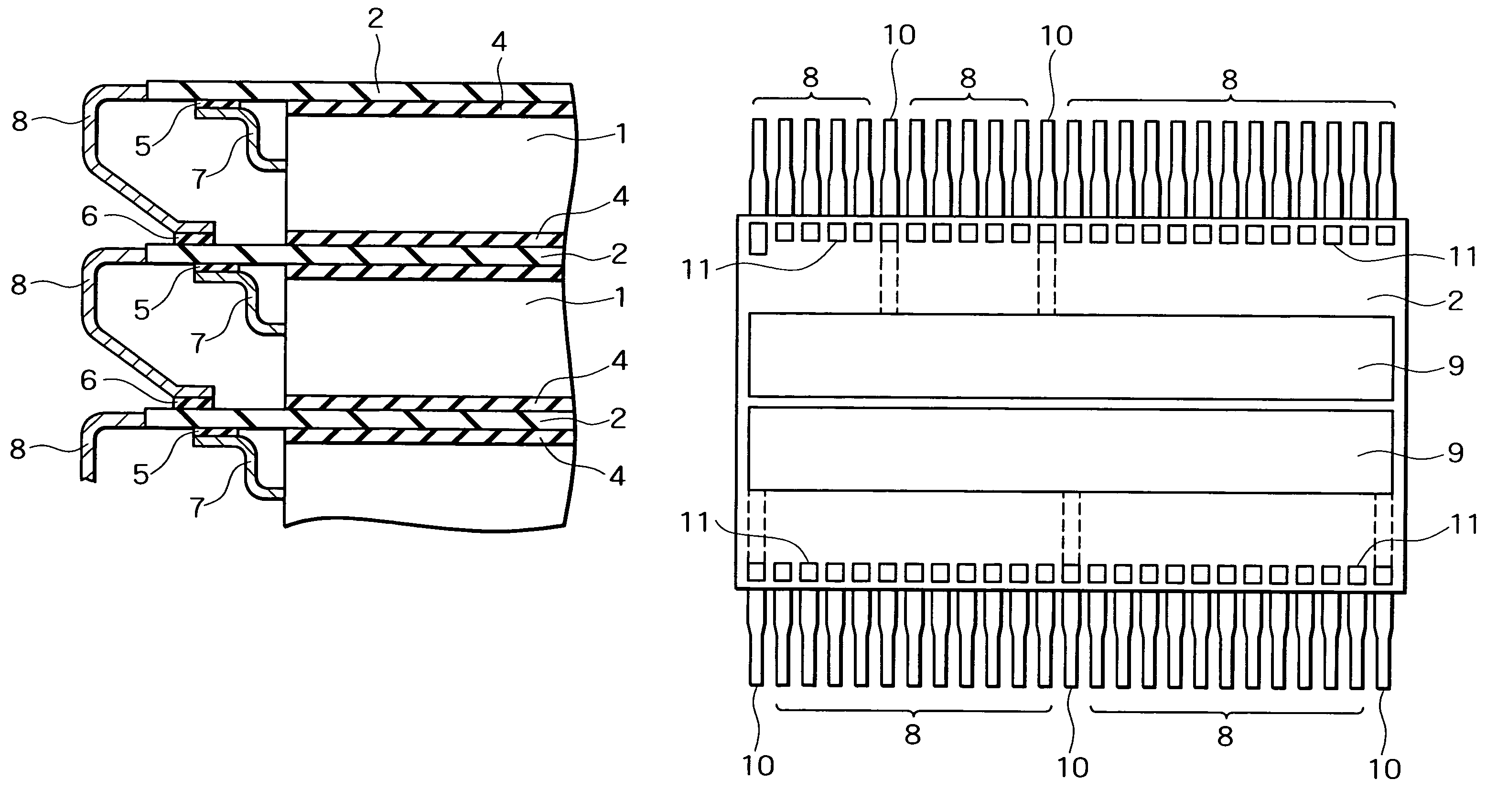
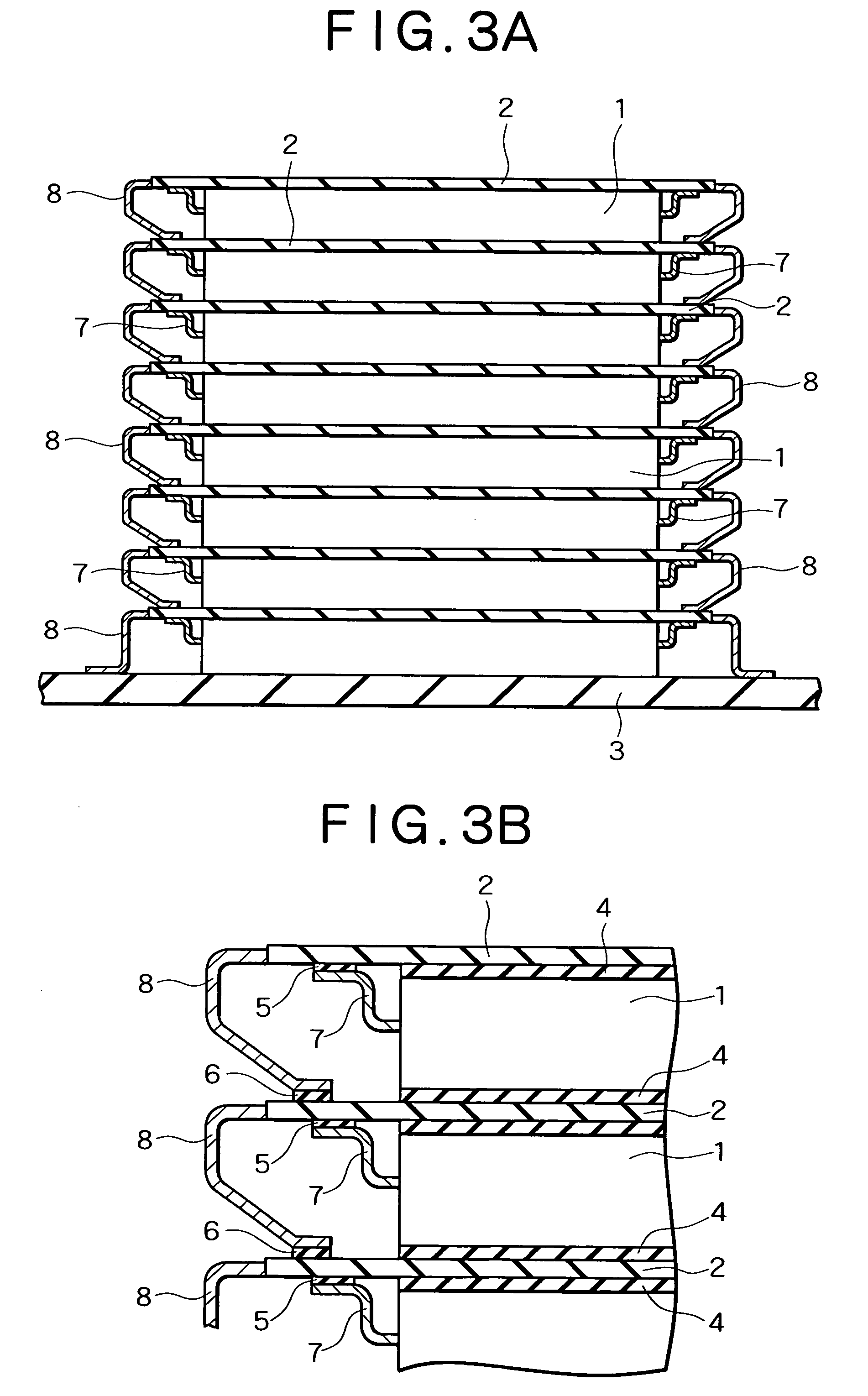
[0023]A stacked memory according to an embodiment of the present invention will be hereinafter described in the concrete with reference to the accompanying drawings. In the stacked memory according to this embodiment, eight interposer substrates with TSOPs mounted thereon are stacked in layers. FIG. 3A is a sectional view showing the stacked memory according to this embodiment, and FIG. 3B is an enlarged sectional view of FIG. 3A. FIG. 4 is a plan view of an interposer substrate 2 shown in FIG. 2. Referring to FIGS. 3A, 3B, and 4, a TSOP 1 is provided with leads 7. Pads 11 and ground layers 9 are formed in each face of the interposer substrate 2. The pads 11 are connected to leads 8 or ground leads 10. The ground layers 9 are connected to the ground leads 10. The ground layers 9 and the ground leads 10 are at the same potential.

[0024]The TSOP 1 is joined to the ground layers 9 of the interposer substrate 2 by a thermosetting conductive resin 4, and leads 7 of the TSOP 1 are joined t...


PUM


Abstract

To mount a TSOP on an interposer substrate, leads provided to the TSOP are joined to pads of the interposer substrate by a thermosetting conductive resin, and the TSOP exclusive of the leads is joined to ground layers formed in the interposer substrate by a thermosetting conductive resin. The interposer substrates with the TSOPs mounted thereon are stacked in eight layers in such a manner that the TSOPs face downward. Then, leads of the upper interposer substrate are joined to pads formed in the rear face of the lower interposer substrate by a thermosetting conductive resin, so that the interposer substrates adjacent in a vertical direction are connected.

Description

BACKGROUND OF THE INVENTION[0001]1. Field of the Invention[0002]The present invention relates to a stacked memory in which a plurality of semiconductor devices are stacked and a manufacturing method thereof. In particular, the present invention relates to a stacked memory used in a harsh environment and a manufacturing method thereof.[0003]2. Description of the Related Art[0004]A stacked memory is composed of a plurality of stacked semiconductor devices, each of which is packaged in a CSP (Chip Size Package), a TSOP (Thin Small Outline Package), or the like. The stacked memory is mounted on a motherboard together with other electronic components to compose a semiconductor memory device or the like. The semiconductor memory device in which the stacked memory is installed, for example, does not need a mechanical drive section and rotation section, which are necessary in a magnetic tape recorder and a hard disk, and operates at high speed with low power consumption. Thus, it is conside...

Claims


Application Information

Patent Timeline
Patent Type & Authority Patents(United States)
IPC IPC(8): H01L23/48H01L25/10H01L25/11H01L25/18H05K1/14H05K3/32H05K3/34
CPCH01L25/105H05K1/141H05K1/144H05K1/145H05K3/321H05K3/3421H05K2201/0397H05K2201/10477H05K2201/10515H05K2201/10689H05K2201/10969H01L2225/1029H01L2225/107H01L2924/0002H01L2924/00
Inventor EBIHARA, NOBUAKISUZUKI, NAOSHI
Owner NEC TOSHIBA SPACE SYST
Why Eureka
Try Eureka