
Analog integrated circuit layout design

an integrated circuit and layout technology, applied in the field of integrated circuit layout design, can solve the problems of time-consuming process, assumption of circuit schematic fixation, and no tool available to automate the overall process

Active Publication Date: 2006-11-21
CADENCE DESIGN SYST INC
View PDF4 Cites 8 Cited by
  • Summary
  • Abstract
  • Description
  • Claims
  • Application Information

AI Technical Summary

Benefits of technology

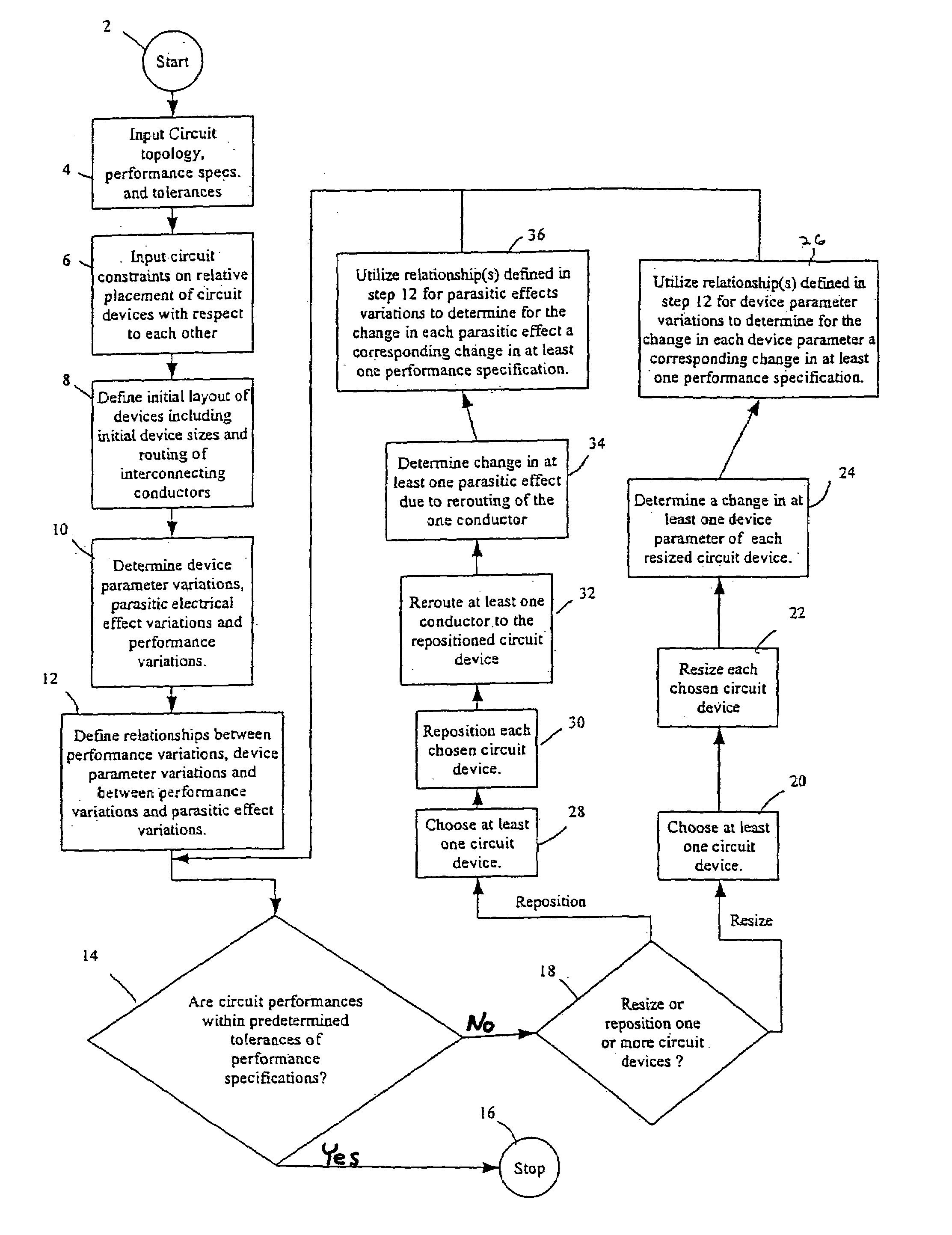
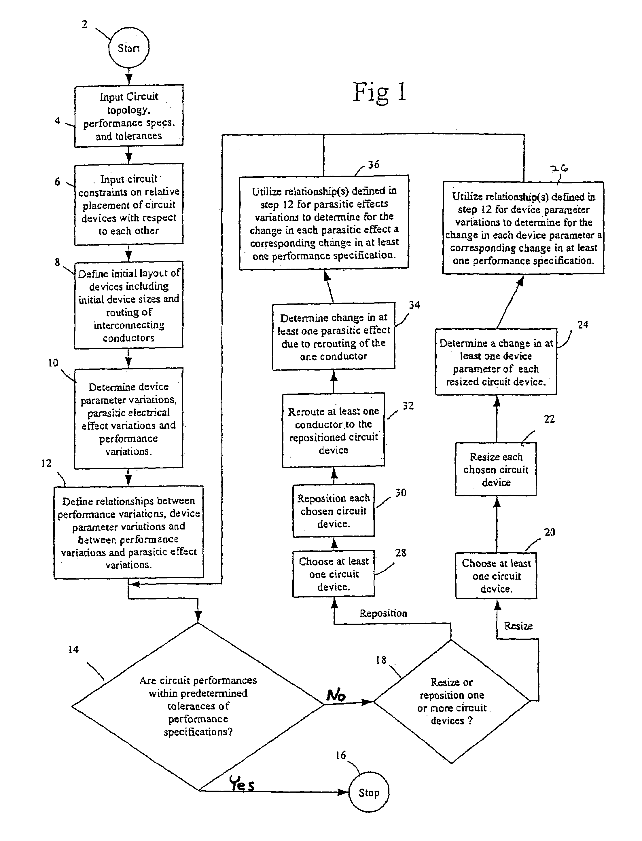
[0014]Lastly, the invention is an automated analog integrated design method that includes: (a) defining performance specifications for a circuit formed from a plurality of interconnected circuit devices; (b) defining at least one constraint on the relative placement of each circuit device with respect to at least one other circuit device; (c) laying out the circuit devices subject to each constraint, wherein each circuit device is assigned a size that establishes at least one device parameter therefor; (d) routing conductors to electrically interconnect the laid out circuit devices whereupon the routing of each conductor establishes an electrical parasitic effect therefor; (e) determining performances for the circuit from the layout of the circuit devices and the routing of the conductors; (f) defining a relationship for each performance, device parameter pair; (g) defining a relationship for each performance, parasitic effect pair; (h) if at least one performance is not within a predetermined tolerance of the corresponding performance specification, choosing one circuit device; (i) randomly resizing or repositioning the chosen circuit device; (j) in response to resizing the one circuit device, repeating steps (h) and (i) after determining a change in at least one performance for the one circuit device utilizing at least one relationship defined in step (f); and (k) in response to repositioning the one circuit device, repeating steps (h) and (i) after determining a change in at least one performance for the one circuit device utilizing at least one relationship defined in step (g).

Problems solved by technology

This process is time consuming and is usually guided only by a designer's experience and expert knowledge about the circuit and layout.
Although separate analog layout tools and circuit synthesis tools are available, heretofore no tool has been available to automate the overall process.
A drawback of existing layout approaches is that they all assume the circuit schematic is fixed when laying out the circuit devices.
So, if one intermediate placement of a circuit device or the routing of an interconnecting conductor violates one performance specification, the entire design is marked as costly or infeasible.

Method used


Image

  • Analog integrated circuit layout design
  • Analog integrated circuit layout design
  • Analog integrated circuit layout design

Examples


Embodiment Construction

[0022]The present invention will be described with reference to the accompanying figures where like reference numbers correspond to like elements.

[0023]The present invention is a method which is desirably embodied in computer readable program code which executes on a processor of a computer system, e.g., a stand-alone or networked computer or workstation, that includes a computer storage, an input / output system, a media drive, such as a disk drive, CD ROM drive, etc., and a computer-usable storage medium capable of storing the computer readable program code that embodies the present invention. Under the control of the computer readable program code, the processor is capable of configuring and operating the computer system in a manner to implement the present invention. Computer systems of the type described above are well known in the art and are not described herein for purpose of simplicity.

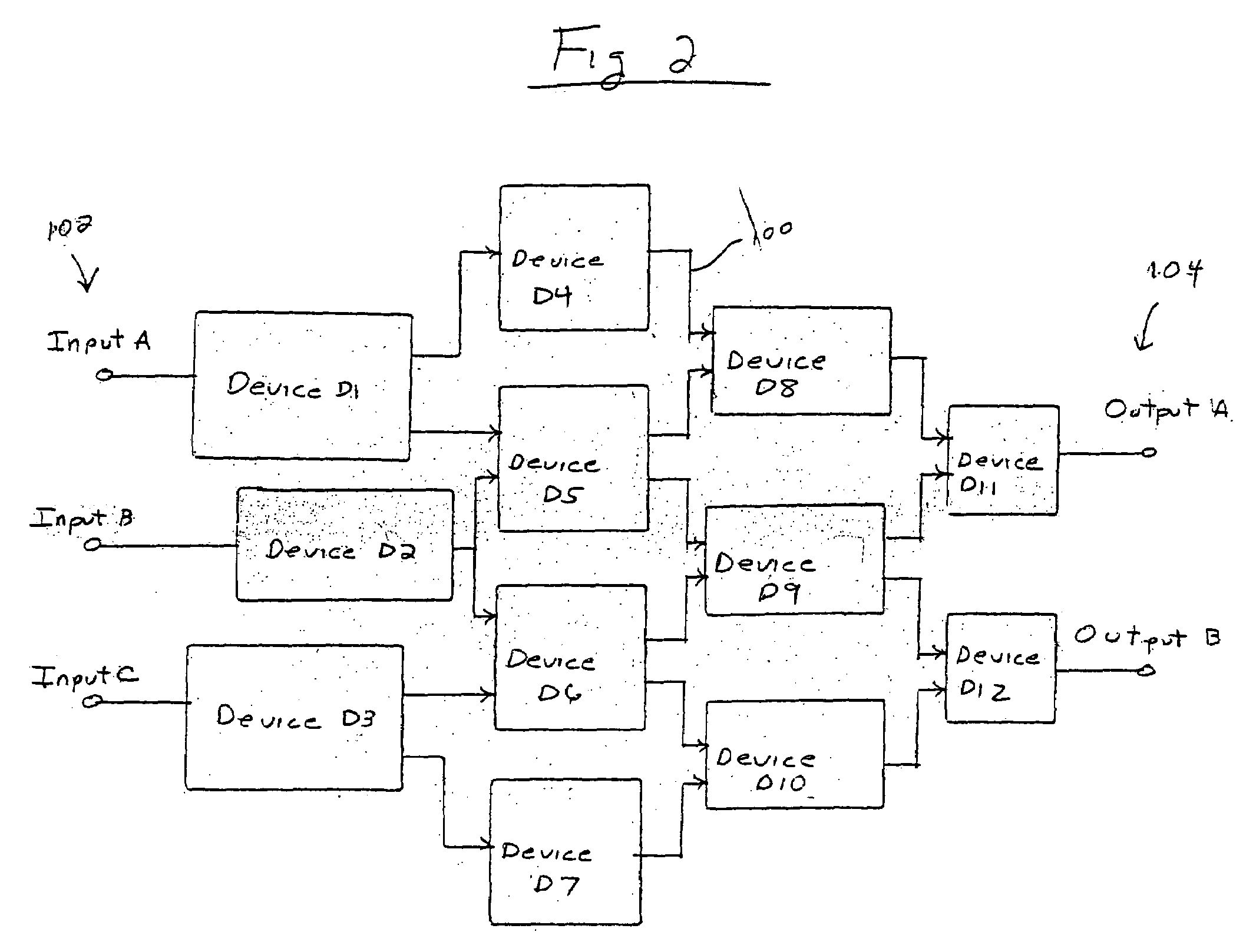
[0024]With reference to FIGS. 1 and 2, the method begins by advancing from a start step 2 t...


PUM


Abstract

In an automated integrated circuit design, if the performances of a layout of circuit devices are not within predetermined tolerances of performance specifications, at least one of the circuit devices is resized or repositioned and an updated value of a device parameter for each resized or repositioned circuit device is determined. A difference between the initial and updated value of each device parameter is then determined and each difference is combined with a ratio formed from changes in the value of one of the device parameters and changes in the value of one of the performances affected by the device parameter. The result of this combination is then combined with the initial value of the performance to determine an updated value therefor.

Description

CROSS REFERENCE TO RELATED APPLICATIONS[0001]This application claims priority from U.S. Provisional Patent Application Ser. No. 60 / 395,156, filed Jul. 11, 2002.BACKGROUND OF THE INVENTION[0002]1. Field of the Invention[0003]The present invention relates to integrated circuit design, and, more particularly, to the automated design of radio frequency and high speed analog integrated circuits.[0004]2. Description of Related Art[0005]The electrical design and physical implementation of integrated circuits, especially radio frequency and high speed analog circuits, are tightly coupled. To this end, parasitic electrical effects resulting from the routing of conductors to interconnect circuit devices must be taken into consideration during front-end electrical synthesis. On the other hand, the back-end layout of circuit devices must be carried out in such a way that target performance specifications are guaranteed to be met. In practice, several iterations between circuit design and layout...

Claims


Application Information

Patent Timeline
Patent Type & Authority Patents(United States)
IPC IPC(8): G06F17/50
CPCG06F17/5063G06F17/5068G06F30/36G06F30/39
Inventor ZHANG, GANGDENGI, ENIS AYKUTROHRER, RONALD A.
Owner CADENCE DESIGN SYST INC
Learn More