
Semiconductor memory device for securely retaining data

a memory device and memory technology, applied in the direction of information storage, static storage, digital storage, etc., can solve the problems of data instability, data loss, data loss, etc., and achieve the effect of suppressing data loss

Inactive Publication Date: 2006-11-07
FUJITSU SEMICON LTD
View PDF13 Cites 5 Cited by
  • Summary
  • Abstract
  • Description
  • Claims
  • Application Information

AI Technical Summary

Benefits of technology

"The present invention aims to solve the problem of data loss in nonvolatile semiconductor memory devices that have operating conditions that can destroy data. The invention provides a solution by providing a memory cell and a guarantee cell that can securely retain data as nonvolatile binary data regardless of operating conditions. The invention allows for the automatic writing of read data to the guarantee cell, ensuring that the data is securely retained until a restore operation is completed. Overall, the invention prevents data loss and ensures the safe retention of data in nonvolatile semiconductor memory devices."

Problems solved by technology

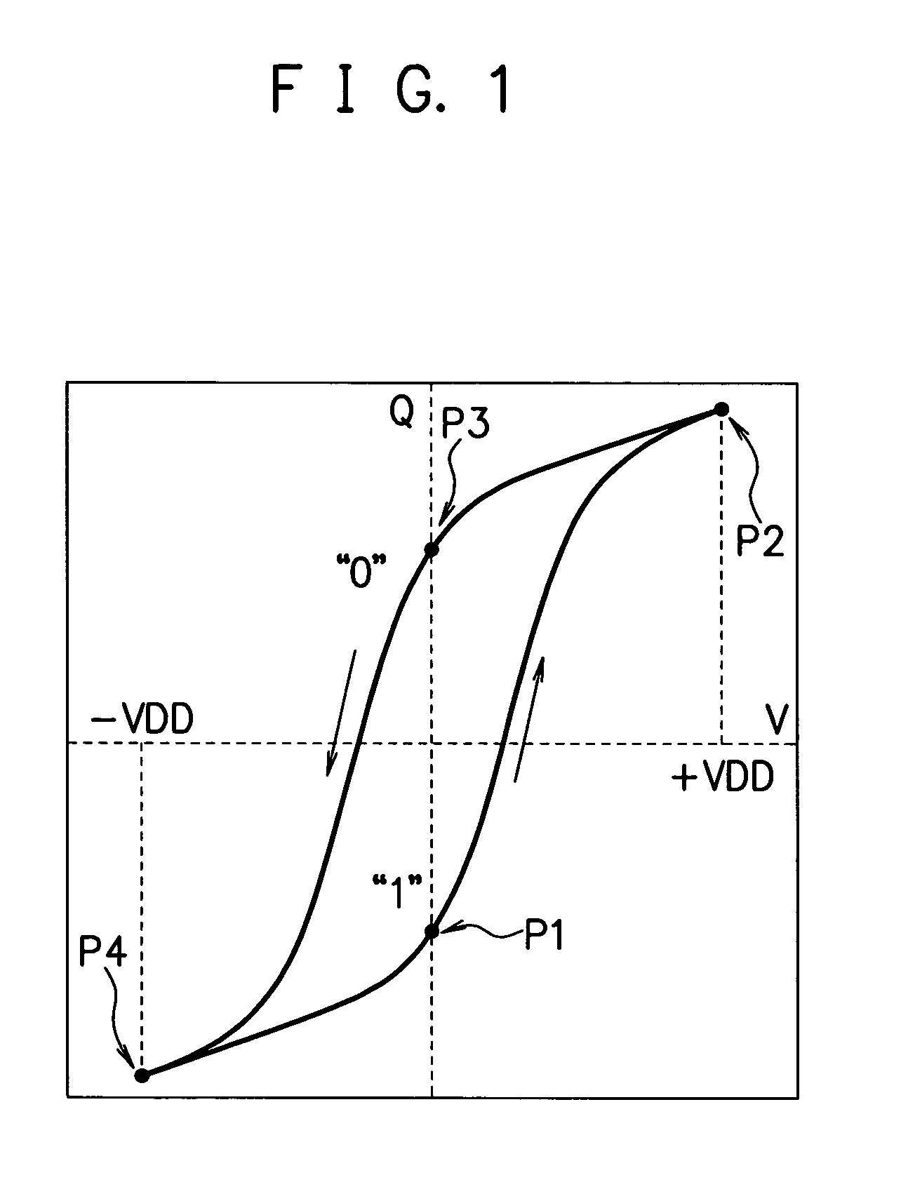
However, reading out of data from the memory cell is destructive reading, which destroys and erases the retained data.
Here, the conventional ferroelectric memory temporarily stores data read out from the memory cell by an electrical signal level (high level or low level) on the bit line until it performs the restore operation in the reading sequence of data, and thus it has instability in a retaining state of data.
In other words, the conventional ferroelectric memory retains data read out from the memory cell by a volatile electric charge, and therefore it has possibility of losing data due to a power cut-off (including a cut-off of power supply, decrease of a power supply voltage), noise interference, swing of potential, and the like.
Furthermore, in the conventional ferroelectric memory, a capacitor and so on for power supply for assuring stable power supply until the reading sequence is completed are provided internally, thereby causing enlargement of circuit area (chip area).
According to the means as described above, data read out from the memory cell during the read sequence can be almost securely written (written back) to the memory cell, but it is not possible to confirm whether the reading sequence of data including the restore operation is completed properly or not.
However, since this method stores the same data in two areas, it needs a memory having storage capacity that is at least double of the amount of data, and its operation is complicated because data has to be synchronized constantly between the pair of memories.

Method used


Image

  • Semiconductor memory device for securely retaining data
  • Semiconductor memory device for securely retaining data
  • Semiconductor memory device for securely retaining data

Examples


first embodiment

[0054

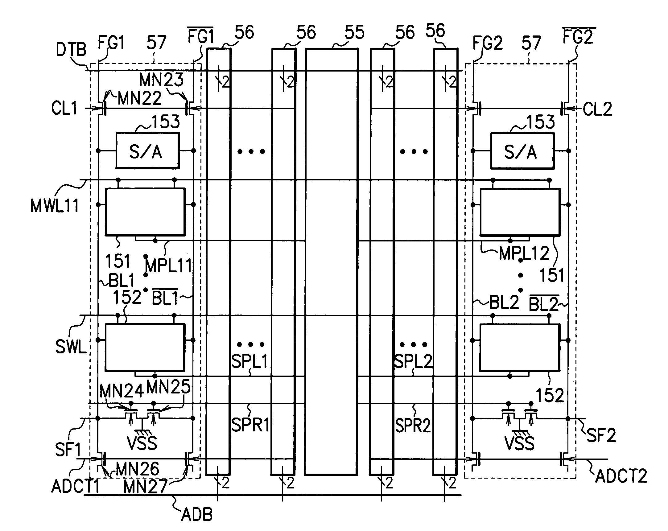
[0055]A semiconductor memory device according to a first embodiment of the present invention suppresses loss of data even when a reading sequence finishes abnormally before a restore operation due to unexpected occurrence of an accident such as a power cut-off. For that purpose, inside the device during a normal state, as soon as data is read out to a bit line from a memory cell retaining the data, the read data is written to and retained in a guarantee cell for retaining data temporarily. Further, address information (address data) is retained as location information for specifying the memory cell from which the data is read out. In case that the reading sequence abnormally finishes before the restore operation, the data retained in the guarantee cell can be written to the memory cell during a startup operation based on the address information.

[0056]FIG. 4 is a block diagram showing a configuration example of a ferroelectric memory device applying the semiconductor memory devi...

second embodiment

[0158

[0159]Next, a second embodiment will be described.

[0160]The ferroelectric memory in the above-described first embodiment, the guarantee cell is added to the bit lines BLi, / BLi to which the memory cells 61 are connected as shown in FIG. 6, and the memory cells 61 and the guarantee cell 62 are always in a state of being connected electrically. Therefore, it is conceivable that increase in capacity due to addition of the guarantee cell 62 causes decrease in operation speed (sense speed) of the sense amplifier 63, or an electric charge discharged during initialization of the guarantee cell 62 charges the bit lines BLi, / BLi.

[0161]Accordingly, a ferroelectric memory to be described below that is application of a semiconductor memory device according to the second embodiment of the present invention allows electrical separation of memory cells and a guarantee cell by transfer gates (transistor) provided on bit lines, and enables control of an electrical connection state between the ...

third embodiment

[0173

[0174]Next, a third embodiment will be described.

[0175]In the case where, for example, one guarantee cell is connected to a bit line to which memory cells are connected, it is conceivable that access concentrates to the guarantee cell to deteriorate cell characteristics in a very short period of time as compared to the memory cells. Accordingly, in a ferroelectric memory that is application of a semiconductor memory device according to the third embodiment of the present invention, a plurality of guarantee cells are connected to the bit line to which the memory cells are connected, thereby preventing concentration of access to one guarantee cell and suppressing the deterioration of cell characteristics of the guarantee cells.

[0176]The ferroelectric memory that is application of the semiconductor memory device according to the third embodiment of the present invention is configured similarly to the ferroelectric memory according to the above-described first and second embodiment...


PUM


Abstract

To a bit line to which a memory cell having a ferroelectric capacitor is connected, a guarantee cell having a ferroelectric capacitor is connected. During a read operation of data from the memory cell, data is read out from the memory cell, and the data read out from the memory cell by destructive reading is written automatically to the guarantee cell, so that the data is retained securely as nonvolatile binary data regardless of operating condition, and thus loss of data can be suppressed.

Description

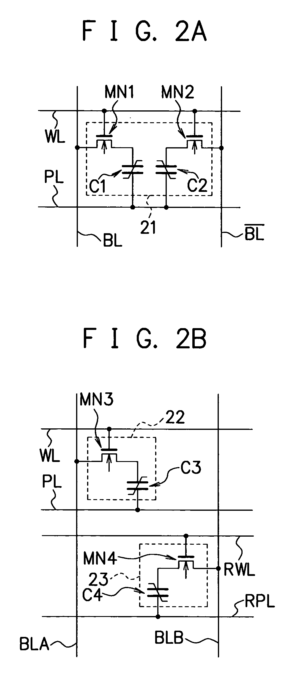
[0001]This nonprovisional application is a continuation application of and claims the benefit of International Application No. PCT / JP03 / 03317, filed Mar. 19, 2003. The disclosure of the prior application is hereby incorporated herein in its entirety by reference.TECHNICAL FIELD[0002]The present invention relates to a semiconductor memory device, and is particularly suitable for use in a ferroelectric memory using ferroelectric capacitors in memory cells.BACKGROUND ART[0003]A ferroelectric memory is a nonvolatile semiconductor memory having the same memory cell structure as a DRAM (Dynamic Random Access Memory) but using a ferroelectric capacitor (ferroelectric element) in a part corresponding to a dielectric capacitor in a memory cell of the DRAM. As a memory cell (storage unit of one bit data) of the ferroelectric memory, there are one transistor / one capacitor (1T / 1C) type cell and two transistors / two capacitors (2T / 2C) type cell, as disclosed in Japanese Patent Application Laid-op...

Claims


Application Information

Patent Timeline
Patent Type & Authority Patents(United States)
IPC IPC(8): G11C11/22G11C11/24
CPCG11C11/22
Inventor SUZUKI, HIDEAKI
Owner FUJITSU SEMICON LTD
Learn More