
Method and apparatus for avoiding gated diode breakdown in transistor circuits

a transistor circuit and gated diode technology, applied in pulse generators, pulse manipulation, pulse techniques, etc., can solve problems such as gated diode breakdown, avalanche of current, and impair circuit operation, and achieve the effect of preventing gated diode breakdown

Inactive Publication Date: 2006-11-07
EMOSYN AMERICA
View PDF7 Cites 43 Cited by
  • Summary
  • Abstract
  • Description
  • Claims
  • Application Information

AI Technical Summary

Benefits of technology

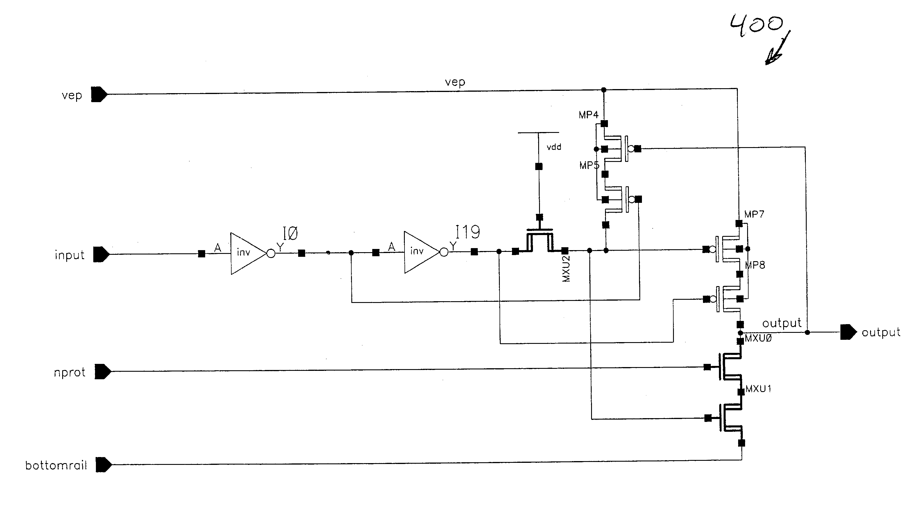
[0010]Generally, an N-channel transistor protection circuit and method are disclosed that prevent gated diode breakdown in N-channel transistors that have a high voltage on their drain. The disclosed N-channel protection circuit may be switched in a high voltage mode between a high voltage level and a bottom rail voltage. According to one aspect of the invention, a high voltage conversion circuit prevents gated diode breakdown in N-channel transistors by dividing the high voltage across two N-channel transistors, MXU0 and MXU1, such that no transistor exceeds the breakdown voltage, Vbreakdown. Generally, the present invention creates an intermediate voltage to drive the top N-channel transistor, MXU0.

Problems solved by technology

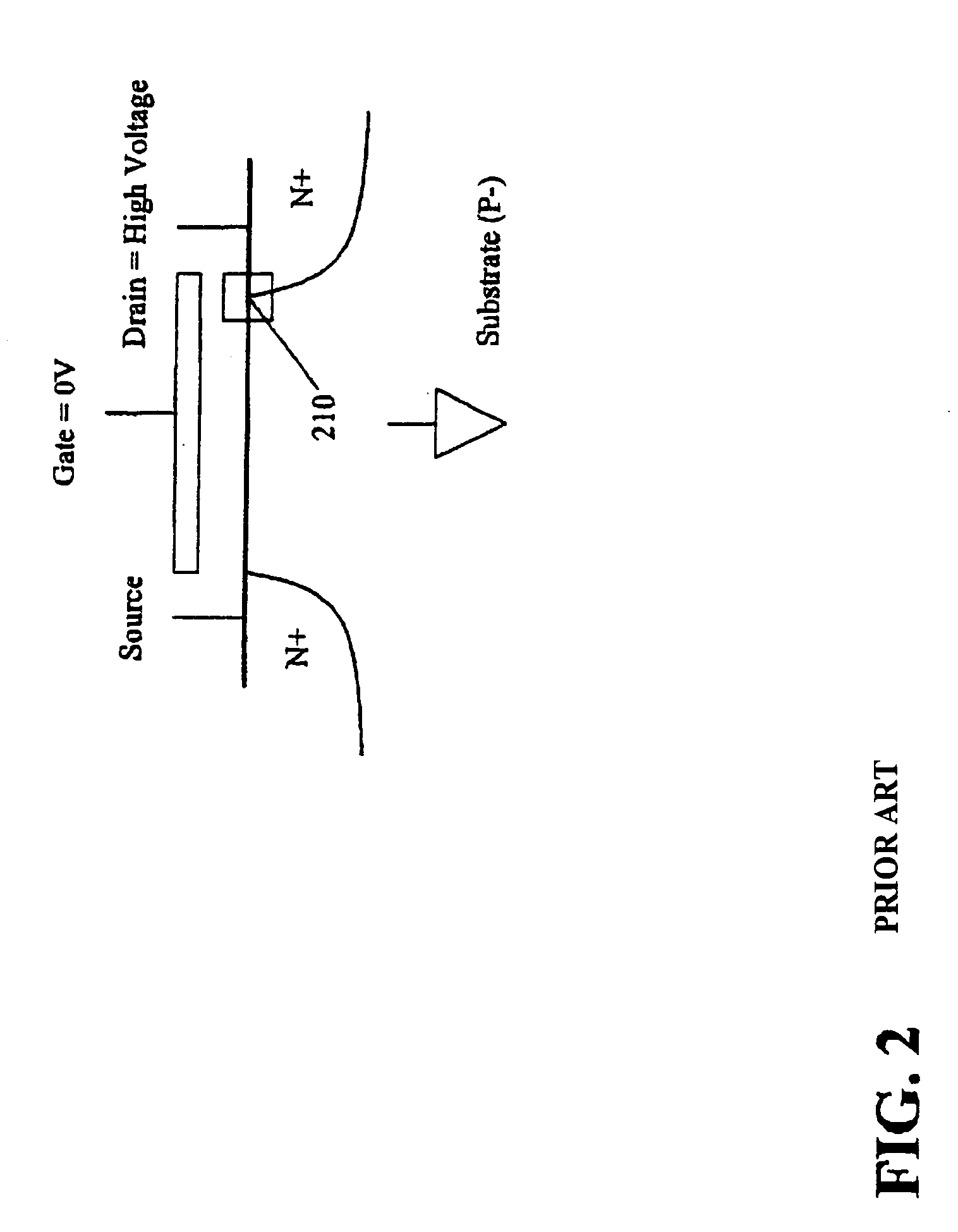
The transistor MXU1 is off in this state, but the high voltage applied to the drain can cause the reverse biased diode from the drain to the P-substrate to break down (right under the gate where the field is the highest), causing an avalanche of current and impairing circuit operation.
In one particular process, a drain voltage on the order of 10 volts has been observed to cause a gated diode breakdown.
For some applications, however, it is necessary, to switch between an output voltage of Vdd and the high voltage level of 10 or 12 volts, which is not possible with the cascaded transistor implementation shown in FIG. 3.

Method used


Image

  • Method and apparatus for avoiding gated diode breakdown in transistor circuits
  • Method and apparatus for avoiding gated diode breakdown in transistor circuits
  • Method and apparatus for avoiding gated diode breakdown in transistor circuits

Examples


Embodiment Construction

[0017]The present invention provides an N-channel protection circuit 400, discussed further below in conjunction with FIG. 4, that prevents gated diode breakdown in N-channel transistors that have a high voltage on their drain, and provides greater flexibility on the output voltages that may be obtained. The high voltage conversion circuit 400 prevents gated diode breakdown in N-channel transistors by dividing the high voltage such that no transistor exceeds the breakdown voltage, Vbreakdown. Generally, the present invention creates an intermediate voltage that is below the high voltage level, Vep, to drive the top N-channel transistor MXU0.

[0018]FIG. 4 illustrates a high voltage conversion circuit 400 incorporating features of the present invention. As shown in FIG. 4, the high voltage conversion circuit 400 includes sets of pairs of transistors, MP4 and MP5, MP7 and MP8, and MXU0 and MXU1, in a similar manner to the modified high voltage conversion circuit 300 of FIG. 3. In order ...


PUM


Abstract

An N-channel transistor protection circuit and method are disclosed that prevent gated diode breakdown in N-channel transistors that have a high voltage on their drain. The disclosed N-channel protection circuit may be switched in a high voltage mode between a high voltage level and a lower rail voltage. A high voltage conversion circuit prevents gated diode breakdown in N-channel transistors by dividing the high voltage across two N-channel transistors, MXU0 and MXU1, such that no transistor exceeds the breakdown voltage, Vbreakdown. An intermediate voltage drives the top N-channel transistor, MXU0. The top N-channel transistor, MXU0, is gated with a voltage level that is at least one N-channel threshold, Vtn, below the high voltage level, Vep, using the intermediate voltage level, nprot. The drain voltage of MXU0 will be at least one N-channel threshold, Vtn, lower than the input voltage level, nprot, and the drain voltage Vd of the bottom N-channel transistor, MXU1, is limited to less than the breakdown voltage, Vbreakdown.

Description

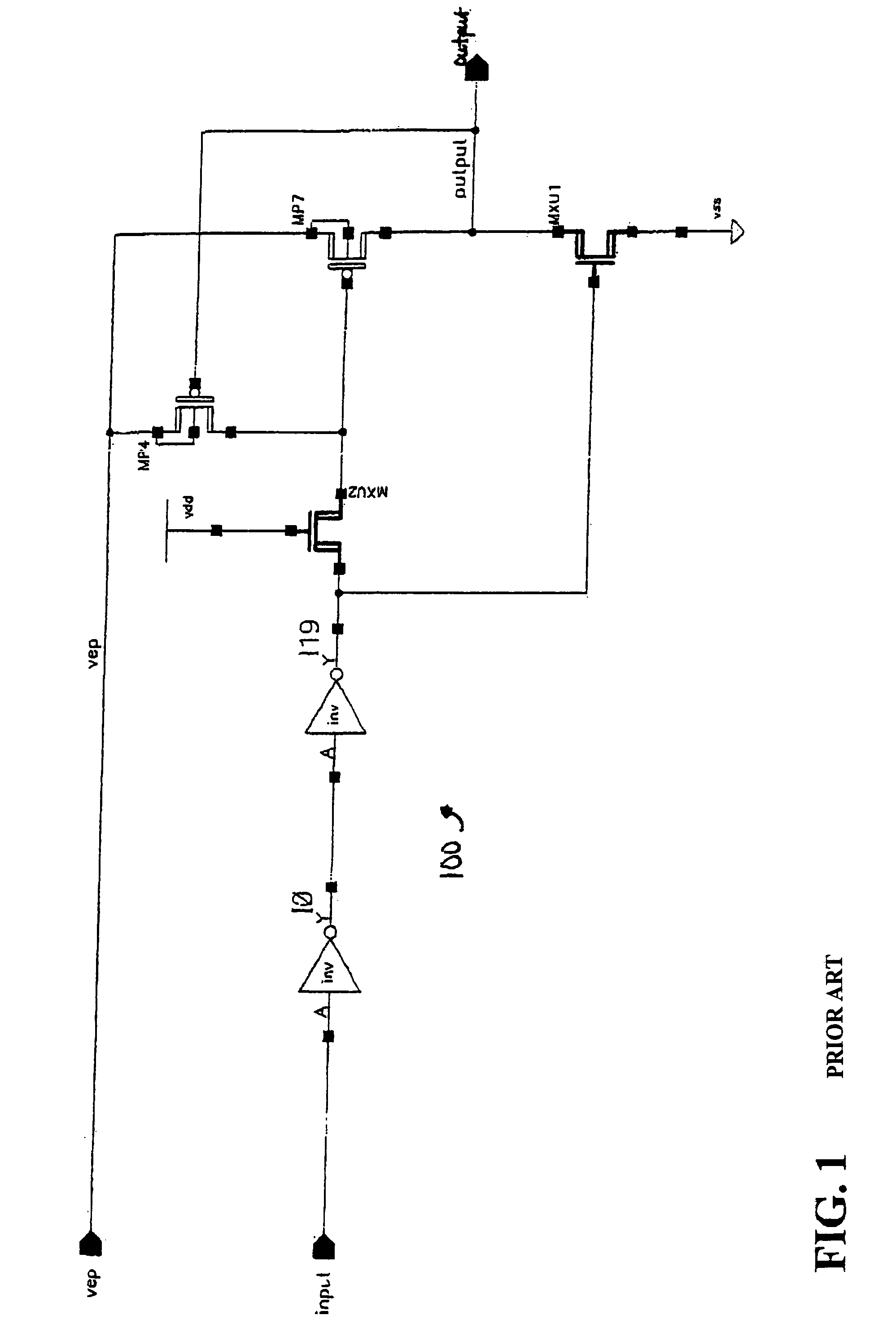
FIELD OF THE INVENTION[0001]The present invention relates generally to a method and apparatus for protecting transistors in a circuit, and more particularly, to a method and apparatus for preventing gated diode breakdown in a voltage conversion circuit.BACKGROUND OF THE INVENTION[0002]Many semiconductor circuits require the switching of high voltages. For example, non-volatile memory devices require voltages to erase and program the memory device that are significantly higher than the voltages needed for other device functions, such as reading data from the memory or communicating with other semiconductor circuits. Thus, semiconductor circuits often employ a voltage conversion circuit to provide the high voltage levels required by the non-volatile memory and other associated devices.[0003]FIG. 1 illustrates a conventional high voltage conversion circuit 100. As shown in FIG. 1, the high voltage conversion circuit 100 receives a logical input signal (0 volts to VDD), input, and a vol...

Claims


Application Information

Patent Timeline
IPC IPC(8): H03K5/08H01L27/02H03K3/00H03L5/00
CPCH01L27/0266
Inventor HOLLMER, SHANE C.
Owner EMOSYN AMERICA
Learn More