
Adjusting power consumption of digital circuitry by generating frequency error representing error in propagation delay

a technology of power consumption and frequency error, applied in the field of digital circuitry, can solve the problems of inefficient power consumption, unacceptably slow performance, affecting the power consumption of the device,

Active Publication Date: 2006-10-31
WESTERN DIGITAL TECH INC
View PDF27 Cites 182 Cited by
  • Summary
  • Abstract
  • Description
  • Claims
  • Application Information

AI Technical Summary

Problems solved by technology

In some computing devices, the propagation delays through certain critical paths of the digital circuitry that must remain within prescribed thresholds for proper operation affect the power consumption of the device.
However, operating all of the computing devices at a predetermined supply voltage to account for worst case conditions leads to inefficient power consumption for the majority of the devices that could operate with acceptable performance using a lower supply voltage.
However, for applications where limiting the clocking frequency leads to unacceptably slow performance, acceptable propagation delay is achieved by increasing the supply voltage.
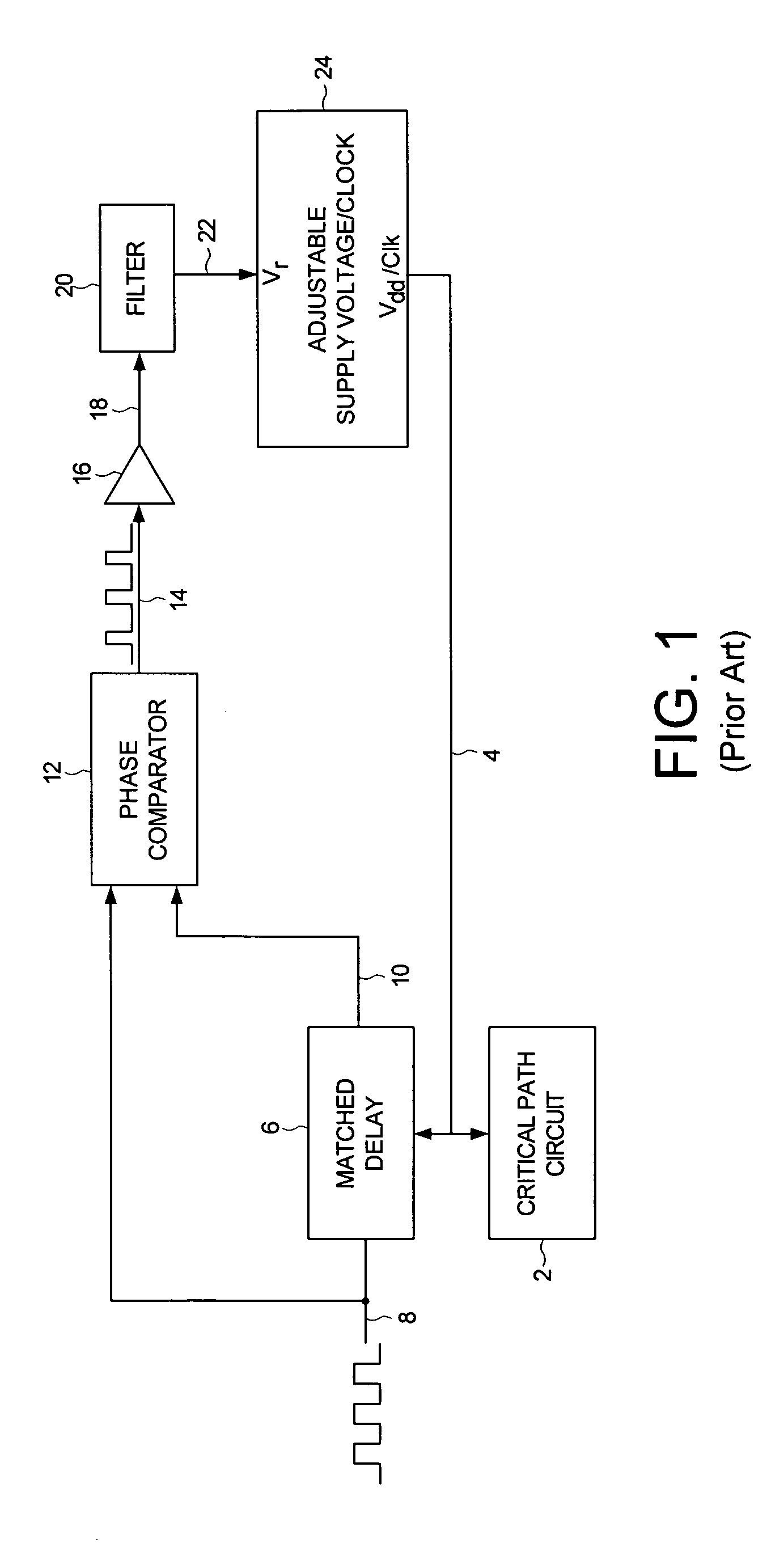
There are a number of drawbacks with the prior art phase comparison technique for measuring the error in propagation delay in order to adjust the supply voltage and / or clocking frequency of digital circuits.
This technique requires the input signal 8 be generated with a period equal to the target propagation delay resulting in design limitations, for example, if the critical path changes relative to the mode of operation or if there are two critical paths with different propagation delays operating simultaneously.
Output rise and fall time errors, impedance, differential delays of the circuitry between rise and fall times, and so forth, all contribute errors in the proportionality constant, and add voltage conversion offsets.
As the target propagation delay through the critical path circuit 2 decreases for higher performance circuits, the delay gets closer to the operating speeds of the digital gates and the proportionality and offset problems are magnified.
Since the highest performance circuits (which require minimal gate delays) consume the most power, the benefit of optimizing power consumption is even more apparent, yet the conversion errors are at their worst for these circuits because the frequency needed to measure the propagation delay is closest to the gate speed limits.
Still further, if the clocking frequency of the digital circuitry is adjusted (e.g., to facilitate different operating modes or to optimize power consumption), non-linearities between the frequency of the input signal 8 and the target reference signal leads to additional voltage errors.
Since power and speed are proportional to the square of the supply voltage of a digital circuit, these introduced voltage errors multiply the power and speed error significantly.
Yet another drawback with the '735 patent is that the period of the input signal 8 must be appropriately selected relative to the propagation delay of the critical path circuit 2 so that the phase shift at the output 10 of the matched delay circuit 6 has sufficient range while timely updating the output of the phase comparator 12.
This problem is exacerbated if a device has a number of critical path circuits that may be enabled at different times, wherein the propagation delay varies significantly between each critical path circuit requiring a corresponding change in the periodic input signal 8.
Still further, a control loop implemented with the prior art phase comparison technique exhibits poor transient response requiring additional margin to ensure proper operation of the device under all operating conditions.

Method used


Image

  • Adjusting power consumption of digital circuitry by generating frequency error representing error in propagation delay
  • Adjusting power consumption of digital circuitry by generating frequency error representing error in propagation delay
  • Adjusting power consumption of digital circuitry by generating frequency error representing error in propagation delay

Examples


Embodiment Construction

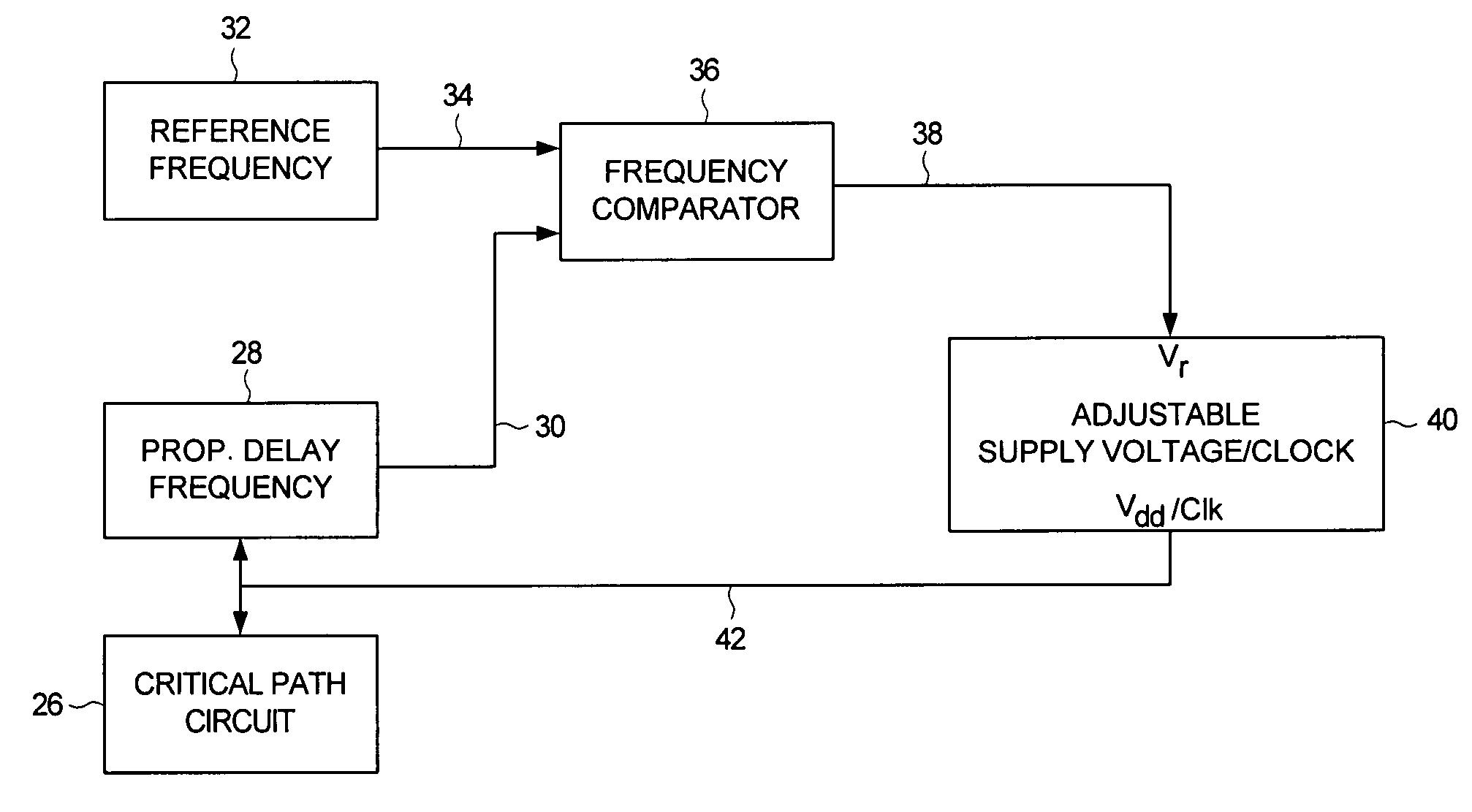
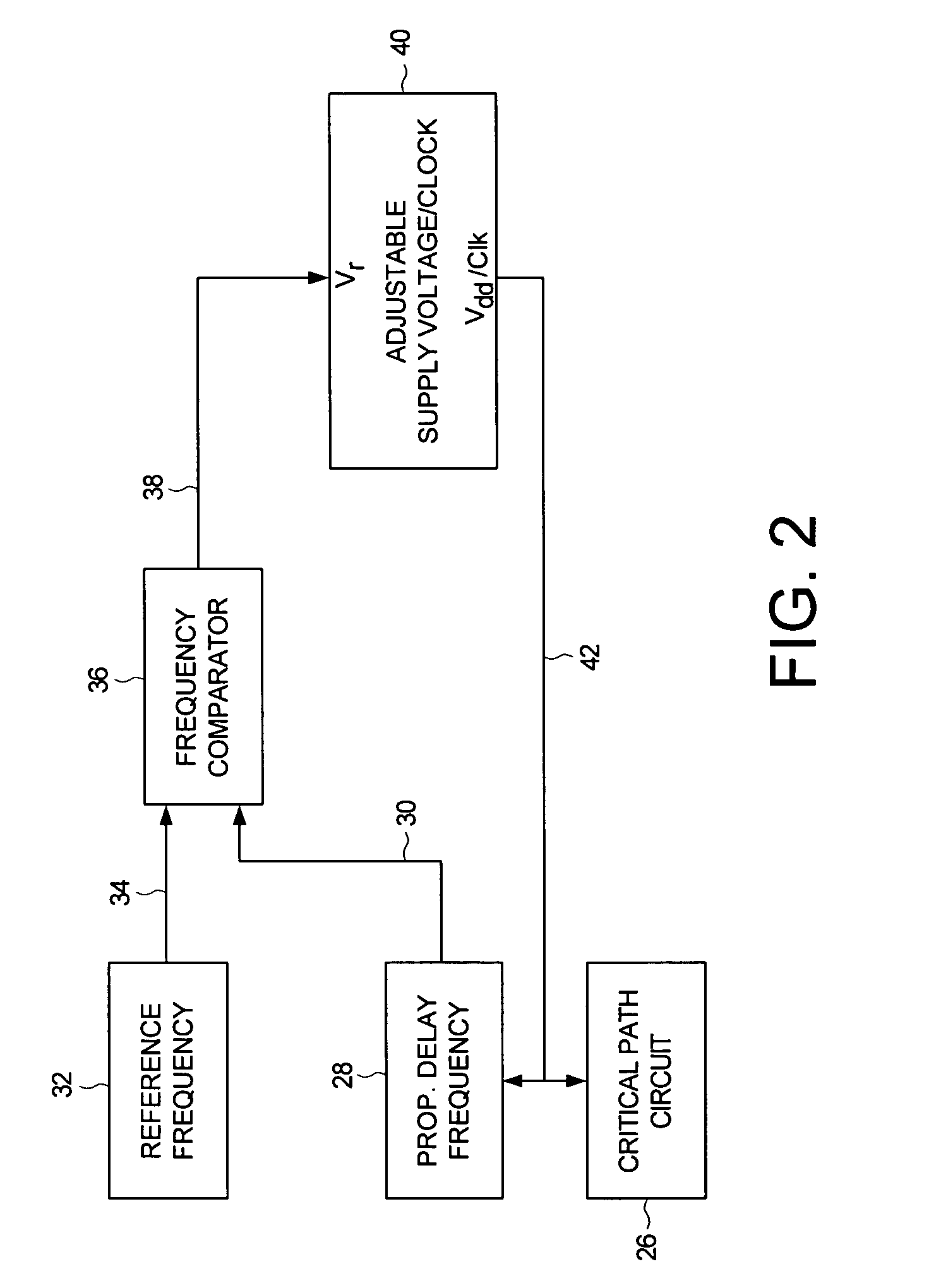
[0031]FIG. 2 shows a computing device according to an embodiment of the present invention comprising digital circuitry including a critical path circuit 26, and a propagation delay circuit 28 for generating a propagation delay frequency 30 representing a propagation delay of the critical path circuit 26. The computing device further comprises a frequency generator 32 for generating a reference frequency 34 and a frequency comparator 36 for generating a frequency error signal 38 representing a difference between the reference frequency 34 and the propagation delay frequency 30. An adjustable circuit 40, responsive to the frequency error signal 38, adjusts at least one of a supply voltage and a clocking frequency 42 applied to the critical path circuit 26.

[0032]Adjusting the supply voltage and / or clocking frequency in response to a frequency error signal representing the error in propagation delay overcomes many of the drawbacks associated with the prior art phase comparison technique...


PUM


Abstract

A method and apparatus is disclosed for adjusting at least one of a supply voltage and a clocking frequency applied to digital circuitry of a computing device, wherein the digital circuitry comprises a critical path circuit. A propagation delay frequency representing a propagation delay of the critical path circuit is generated, and a frequency error signal is generated representing a difference between a reference frequency and the propagation delay frequency. At least one of the supply voltage and the clocking frequency is adjusted in response to the frequency error signal.

Description

BACKGROUND OF THE INVENTION[0001]1. Field of the Invention[0002]The present invention relates to digital circuitry for computing devices. In particular, the present invention relates to adjusting power consumption of digital circuitry by generating a frequency error representing error in propagation delay.[0003]2. Description of the Prior Art[0004]Reducing power consumption of digital circuitry in computing devices increases battery life in portable applications (such as cellular telephones, portable computers, digital cameras, and the like) in addition to increasing the overall reliability / longevity since reducing power consumption reduces the operating temperature and associated stress on the device. In some computing devices, the propagation delays through certain critical paths of the digital circuitry that must remain within prescribed thresholds for proper operation affect the power consumption of the device. For example, manufactures have imposed certain restrictions on proce...

Claims


Application Information

Patent Timeline
IPC IPC(8): H03L7/06H03L7/00
CPCG06F1/3203G06F1/324G06F1/3296H03L7/0805H03L7/085H03L7/0995Y02B60/1217Y02B60/1285Y02D10/00
Inventor BENNETT, GEORGE J.VASQUEZ, STEVEN R.
Owner WESTERN DIGITAL TECH INC
Learn More