
Capacitor layout technique for reduction of fixed pattern noise in a CMOS sensor

a cmos sensor and layout technique technology, applied in capacitors, solid-state devices, instruments, etc., can solve problems such as fixed pattern noise, and achieve the effect of reducing fixed pattern nois

Inactive Publication Date: 2006-10-17
MICRON TECH INC
View PDF9 Cites 2 Cited by
  • Summary
  • Abstract
  • Description
  • Claims
  • Application Information

AI Technical Summary

Benefits of technology

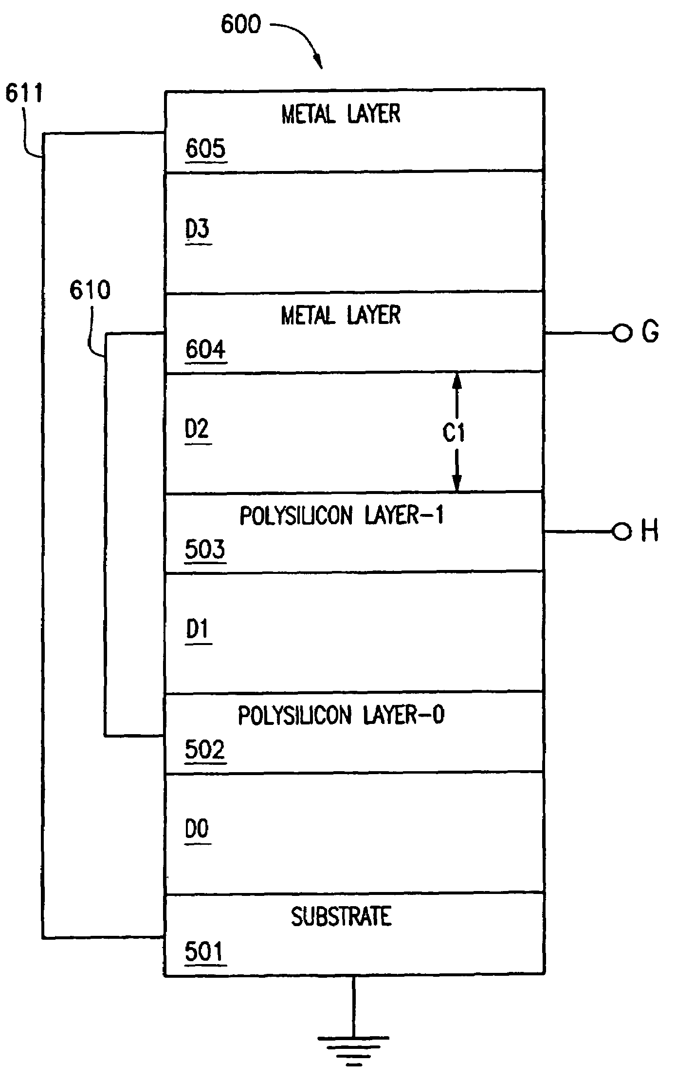
The present invention is about a new capacitor structure for use in a sample-and-hold subcircuit of an APS CMOS imaging system. The new structure shields the most sensitive electrode node between a set of equal potential layers to form a capacitor back plate, which in turn is surrounded by another set of equal potential layers to act as a guard plate connected to ground. This arrangement reduces fixed pattern noise by a factor of eight. Overall, the invention improves the performance of the sample-and-hold subcircuit.

Problems solved by technology

One issue associated with APS CMOS imaging systems is that of fixed pattern noise, which is a type of distortion in the image captured by the imaging system.

Method used


Image

  • Capacitor layout technique for reduction of fixed pattern noise in a CMOS sensor
  • Capacitor layout technique for reduction of fixed pattern noise in a CMOS sensor
  • Capacitor layout technique for reduction of fixed pattern noise in a CMOS sensor

Examples


Embodiment Construction

[0022]One important source of parasitic capacitance arises from the way capacitors, such as sampling capacitors 301, 302 are conventionally fabricated. Now referring to the drawings, where like reference numerals designate like elements, there is shown in FIG. 5 an illustration of an integrated circuit capacitor 500 fabricated in the conventional manner. The capacitor 500 includes a substrate layer 501, which is coupled to ground. Dielectric layer D0, polysilicon layer-0502, dielectric layer D1, and polysilicon layer-1503 are respectively layered above the substrate 501. The capacitor 500 is formed between node-E and node-F. The two polysilicon layers 502, 503, which sandwich dielectric layer D1, serve as the two plates of the capacitor 500, which has a capacitance of C1.

[0023]This traditional method of producing a capacitor 500 provides undesirable electric field interactions at both polysilicon layers 502, 503. More specifically, electric field lines may radiate through the polysi...


PUM


Abstract

A new capacitor architecture includes a front plate of the capacitor formed form a first polysilicon layer. The front plate is surround by a first dielectric layer and a second dielectric layer. The back plate of the capacitor is formed from one layer of a first two-layer conductive structure which surrounds the first dielectric layer and the second dielectric layer. The two-layer conductive structure is an equal potential structure and includes a conductive coupling between the two layers.

Description

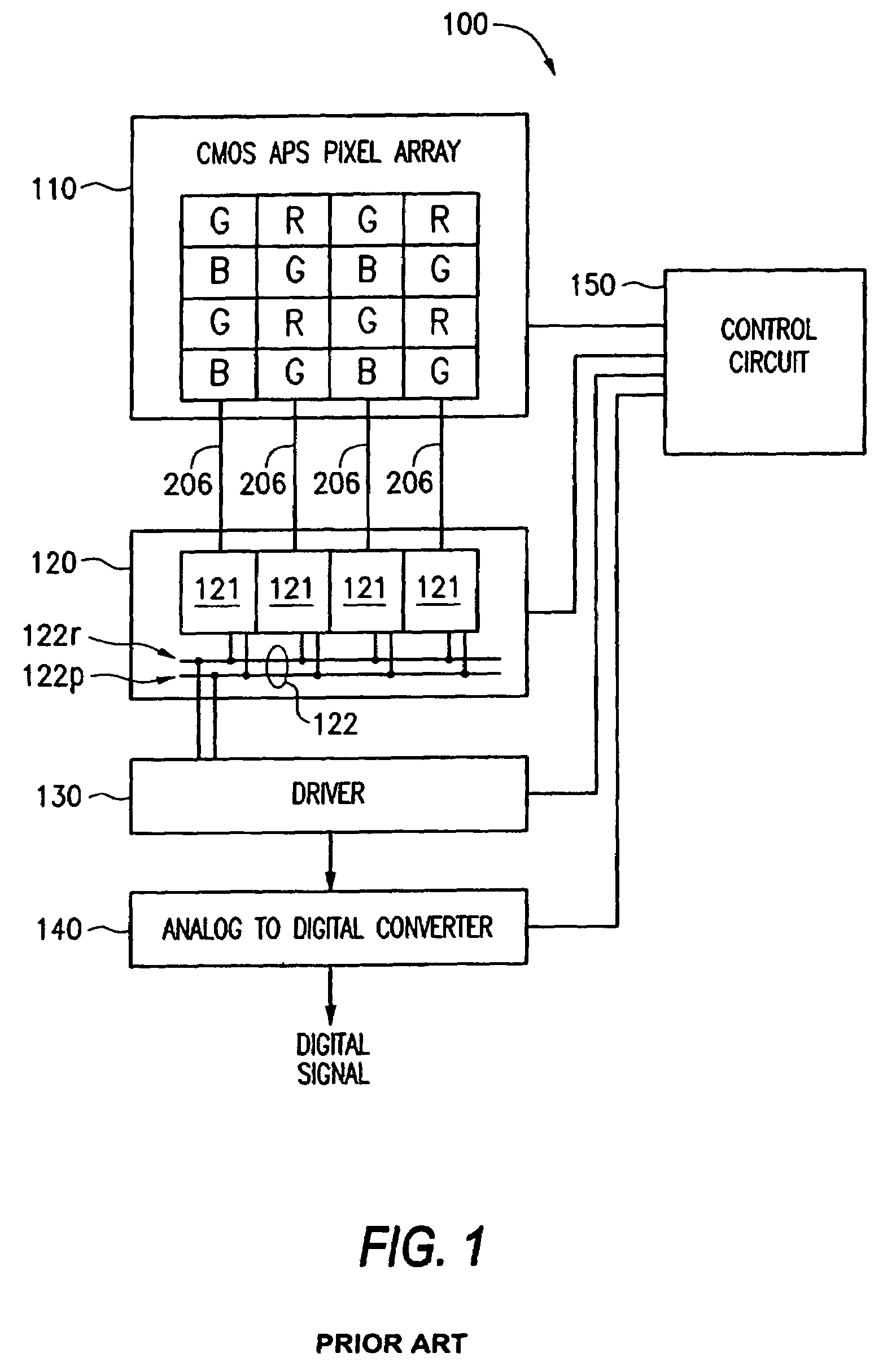
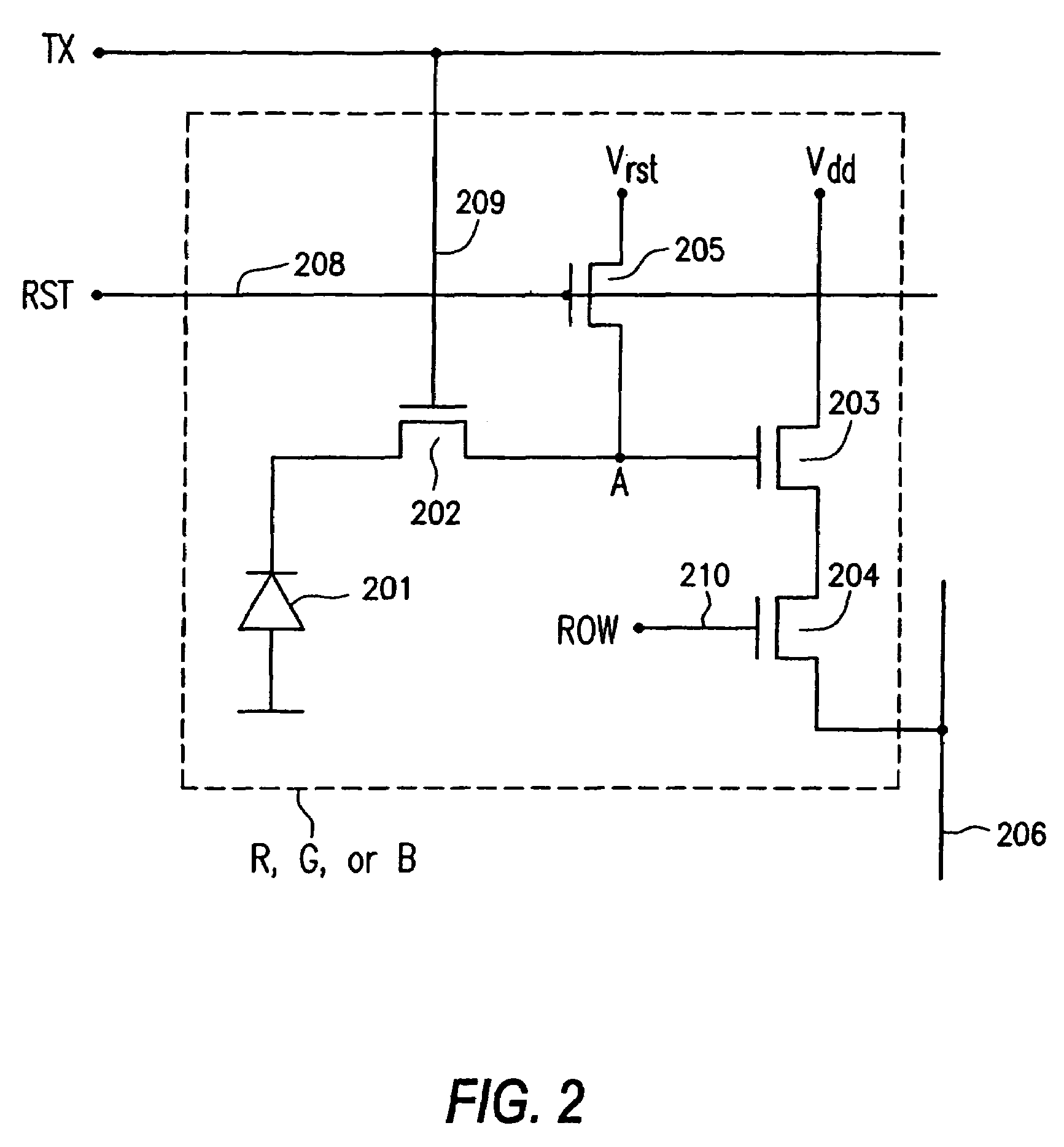
[0001]This application is a continuation of application Ser. No. 10 / 216,804, filed Aug. 13, 2002 now U.S. Pat. No. 6,774,459 (issue fee paid), the subject matter of which is incorporated by reference herein.FIELD OF INVENTION[0002]The present invention relates to a CMOS active pixel sensor system. More specifically, the present invention is directed to a capacitor architecture useful for minimizing fixed pattern noise in a sample-and-hold stage of a CMOS active pixel sensor system.BACKGROUND OF THE INVENTION[0003]FIG. 1 is an illustration of a front-end portion of a color CMOS active pixel sensor (APS) imaging system 100. The system 100 includes a N×M pixel array 110 comprised of pixels R, G, B which are sensitive to red, green, and blue colored light, respectively. The pixels R, G, B are typically arranged in a Bayer pattern, in which alternating rows are comprised of green / red and green / blue pixels in adjacent columns.[0004]Any image focused upon the pixel array 110 causes the pix...

Claims


Application Information

Patent Timeline
Patent Type & Authority Patents(United States)
IPC IPC(8): H01L29/00G06F17/50H01L27/08H01L29/94
CPCH01L27/0805H01L28/40H01L29/94H01L27/14609Y10S438/957
Inventor ROSSI, GIUSEPPE
Owner MICRON TECH INC
Learn More