Jfet charge control device for an imager pixel

a charge control and imager technology, applied in the field of imager devices, can solve the problems of difficult to precisely control the transistors, uncertainty in the amount of charge stored from pixel cell to pixel cell, and the barrier of the mos transistor, so as to reduce the uncertainty of pixel-to-pixel charge, improve image quality, and improve the effect of charge control

Inactive Publication Date: 2005-10-27
MICRON TECH INC
View PDF5 Cites 14 Cited by
  • Summary
  • Abstract
  • Description
  • Claims
  • Application Information

AI Technical Summary

Benefits of technology

[0012] Various embodiments of the invention provide a new pixel design for an imager in which a junction field effect transistor (JFET) transistor is provided in an anti-blooming path during charge integration. Since a JFET transistor does not have an oxide layer below its gate, it has a better defined threshold voltage (Vth) and thus it provides improved charge control for the pixel. Utilizing a JFET transistor as an anti-blooming transistor thus reduces pixel-to-pixel charge uncertainty. The reduction of fixed pattern noise results in improved image quality.

Problems solved by technology

However, there is a problem in using CMOS transistors as barriers in imager pixel cells.
For example, the gate oxide layer can assimilate floating charges that make it difficult to precisely control the transistors.
This deviation leads to an uncertainty in the amount of charge stored from pixel cell to pixel cell since the threshold voltage Vth of each transistor could vary.
The variance of charge storage from pixel cell to pixel cell in an imager array leads to fixed pattern noise (FPN) resulting in diminished image quality because non-uniformity of barrier heights between pixels.
Consequently, the fixed pattern noise for the imager array increases resulting in diminished image quality.
A similar problem exist the gate of the transfer transistor as with the CMOS anti-blooming transistor.

Method used


Image

  • Jfet charge control device for an imager pixel
  • Jfet charge control device for an imager pixel
  • Jfet charge control device for an imager pixel

Examples


Embodiment Construction

[0024] In the following detailed description, reference is made to the accompanying drawings, which are a part of the specification, and in which is shown by way of illustration various embodiments whereby the invention may be practiced. These embodiments are described in sufficient detail to enable those skilled in the art to make and use the invention. It is to be understood that other embodiments may be utilized, and that structural, logical, and electrical changes, as well as changes in the materials used, may be made without departing from the spirit and scope of the present invention. Additionally, certain processing steps are described and a particular order of processing steps is disclosed; however, the sequence of steps is not limited to that set forth herein and may be changed as is known in the art, with the exception of steps or acts necessarily occurring in a certain order.

[0025] The terms “wafer” and “substrate” are to be understood as interchangeable and as including...


PUM


Abstract

A pixel cell that utilizes a JFET transistor, instead of a CMOS transistor, linked to each pixel's photosensor as an anti-blooming and/or transfer transistor to provide an overflow path for electrons during charge integration. Using a JFET transistor reduces charge uncertainty and fixed pattern noise in the imaging system.

Description

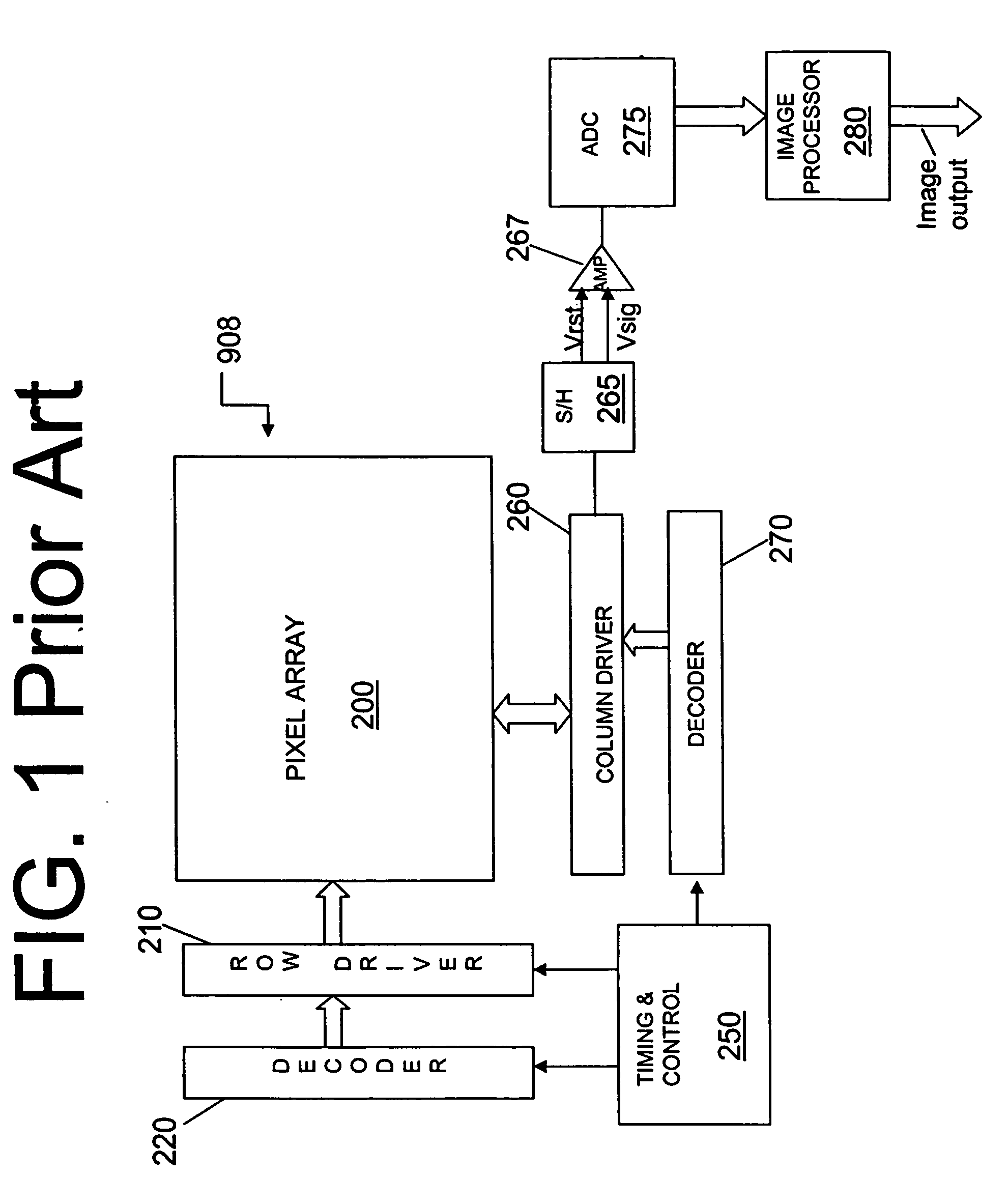
FIELD OF THE INVENTION [0001] The invention relates to imager devices generally and particularly to improving the control and operation of an imager pixel. BACKGROUND OF THE INVENTION [0002] An imager, for example, a CMOS imager includes a focal plane array of pixel cells; each cell includes a photosensor, for example, a photogate, photoconductor or a photodiode overlying a substrate for producing a photo-generated charge in a doped region of the substrate. A pixel uses CMOS transistors, which are a form of metal oxide semiconductor field effect transistor (MOSFET). A readout circuit is provided for each pixel cell and typically includes at least a source follower transistor and a row select transistor for coupling the source follower transistor to a column output line. The pixel cell also typically has a charge storage node, for example, a floating diffusion region which is, in turn, connected to the gate of the source follower transistor. Charge generated by the photosensor is sto...

Claims


Application Information

Patent Timeline
Patent Type & Authority Applications(United States)
IPC IPC(8): H04N3/14H04N5/365H04N5/3745
CPCH04N5/374H04N5/365H04N25/67H04N25/76
Inventor JERDEV, DMITRIAGRANOV, GENNADIY A.
Owner MICRON TECH INC
Why Eureka
Try Eureka