Apparatus and method for driving luminescent display panel

Inactive Publication Date: 2006-10-10
TOHOKU PIONEER CORP
View PDF19 Cites 15 Cited by
  • Summary
  • Abstract
  • Description
  • Claims
  • Application Information

AI Technical Summary

Benefits of technology

[0035]The present invention has been conceived while paying attention to the foregoing problems and aims at providing an apparatus and method for driving a luminescent display panel which can stabilize light-emission luminance of light-emitting elements typified by the previously-described organic EL elements without involvement of adjustment and which can essentially prolong the operating life of the light-emitting elements.
[0050]If the cathode resetting method is adopted for the apparatus for driving the luminescent display panel, a charging voltage corresponding to the bias voltage VM with which the EL elements are initially charged immediately before scanning operation is at all times maintained at a level close to the peak value of the forward voltage Vf of the element. Hence, there can be prevented occurrence of a delay, which would otherwise arise in the time at which the EL elements start illuminating by an initial charging operation. Further, the reverse bias voltage VM does not rise higher than the forward voltage Vf, and hence there is prevented occurrence of excessive illumination damage, which would otherwise be caused by excessive recharging. Consequently, the EL element illuminates optimally instantaneous with commencement of scanning operation. Hence, the quantity of illumination of the EL element can be controlled so as to become substantially constant.
[0051]Even if a rise arises in the forward voltage Vf of the EL element for reasons of long-term use, the quantity of illumination of the EL element is controlled so as to become substantially constant. Hence, a period during which a predetermined quantity of illumination of the EL element can be ensured; that is, the life of the EL element, can be prolonged.
[0052]The reverse bias voltage VM which is controlled so as to become an appropriate value in pursuit of the forward voltage Vf of the EL element is supplied to each of the EL elements connected to the intersections between the driven anode line and the cathode lines not selected for scanning. Hence, there can be effectively inhibited occurrence of crosstalk illumination, which would otherwise be caused by the EL elements. Further, there can be prevented occurrence of a problem of deterioration of display grade of the display panel, which would otherwise be caused by the previously-described leakage phenomenon.
[0053]The foregoing effects similarly apply to variations in a forward voltage due to variations; e.g., in film-growth (deposition) treatment performed at the time of production of an EL element or a change in forward voltage of an EL element, which would otherwise arise according to the color of illumination of the EL element. Hence, a stable and optimized illumination characteristic can be achieved at all times without particular adjustment of an operating point of a circuit.

Problems solved by technology

Consequently, the luminance characteristic of the EL element also deteriorates.
The current / luminance characteristic of the EL element is stable, whereas a voltage / luminance characteristic of the same is unstable.
This eventually presents a problem of a delay arising in start-up of the EL element.
Hence, a limitation is imposed on an electric current, thereby inducing a noticeable delay in the rise and illumination of the EL element.
However, if the value of the reverse bias voltage VM is set excessively high, a so-called leakage phenomenon will arise, thereby deteriorating the display grade of the display panel.
Consequently, a delay arises in the time at which an EL element starts illuminating by means of an initial charging operation using the fixed reverse bias voltage VM, along with a problem of the quantity of illumination of the EL element gradually decreasing.
In other words, a period during which a predetermined quantity of illumination of the EL element can be ensured is shortened, thereby turning into another problem of the life of the EL element becoming essentially short.
Further, a temperature compensation curve does not necessarily match the characteristic of the EL element.
For these reasons, difficulty is encountered in achieving a satisfactory compensation characteristic.
However, in reality, adoption of such a configuration is difficult, thereby posing difficulty in arranging and designing a thermistor.

Method used


Image

  • Apparatus and method for driving luminescent display panel
  • Apparatus and method for driving luminescent display panel
  • Apparatus and method for driving luminescent display panel

Examples


first embodiment

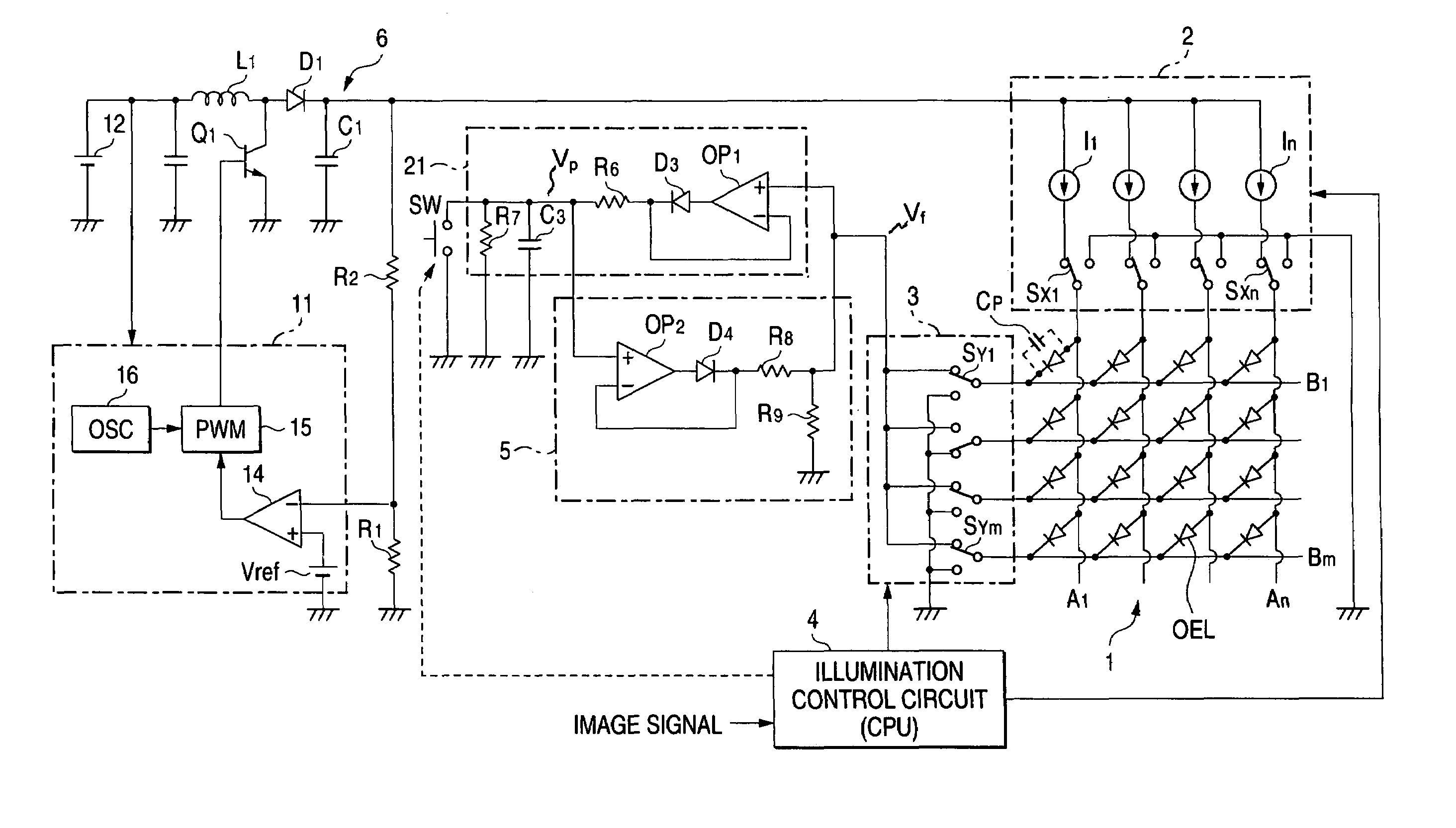
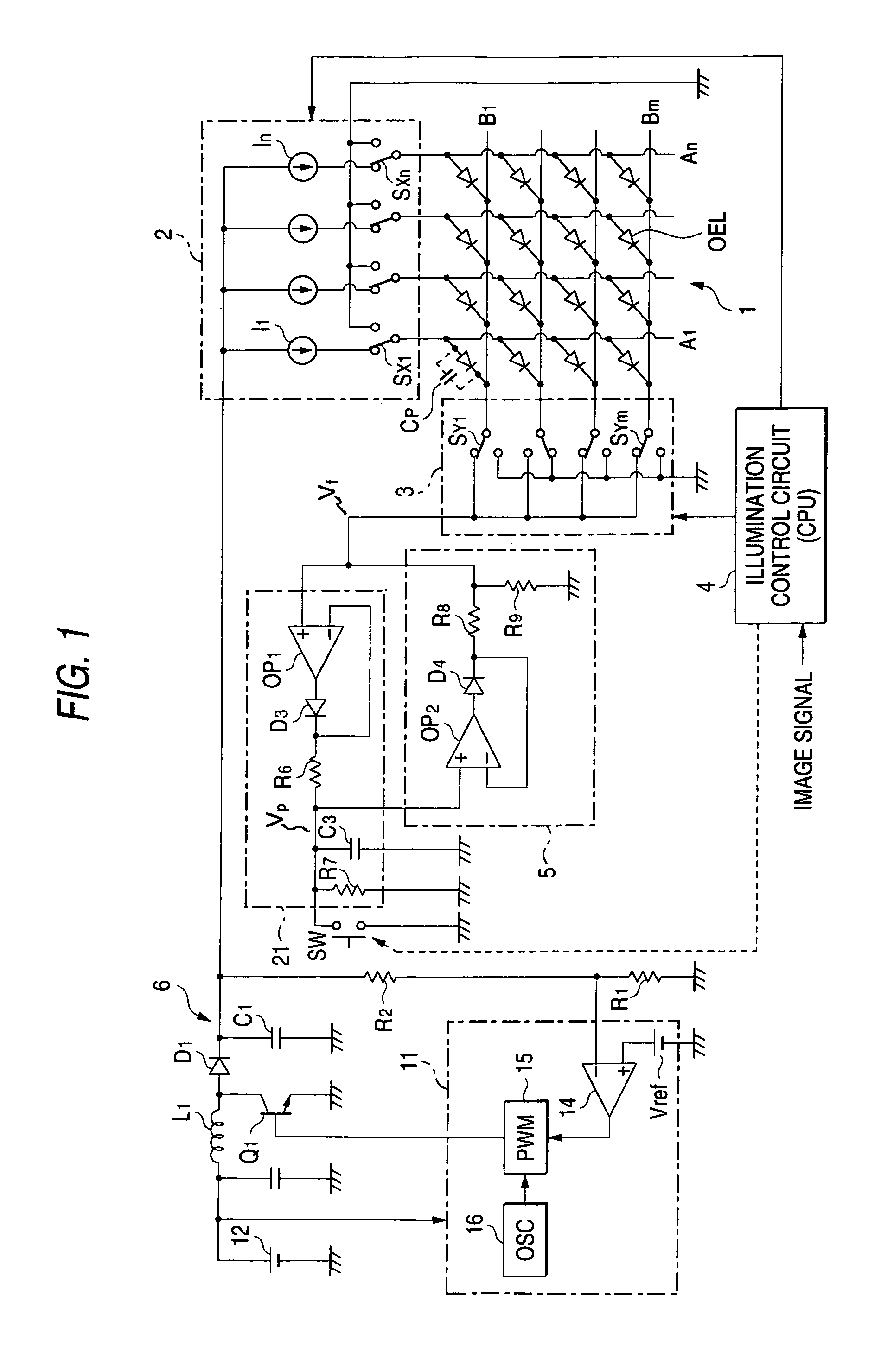
[0062]an apparatus for driving a luminescent display panel according to the invention will be hereinafter described by reference to FIG. 1. In relation to FIG. 1, constituent elements corresponding to those that have already been described and shown in FIG. 6 are assigned the same reference numerals, and their detailed descriptions are omitted, as required. Reference numeral 21 shown in FIG. 1 designates a peak holding circuit. Here, the peak holding circuit 21 is constituted of an operational amplifier OP1, a diode D3, a resistor R6, and a capacitor C3.

[0063]A non-inverse input terminal of the operational amplifier OP1 constitutes an input terminal of the peak holding circuit 21. By way of scanning switches SY1 through SYm in the cathode line scanning circuit 3, the non-inverse input terminal of the operational amplifier OP1 is connected to cathode lines B1 through Bm when in a non-scanning state. An output terminal of the operational amplifier OP1 is connected to an anode of the d...

third embodiment

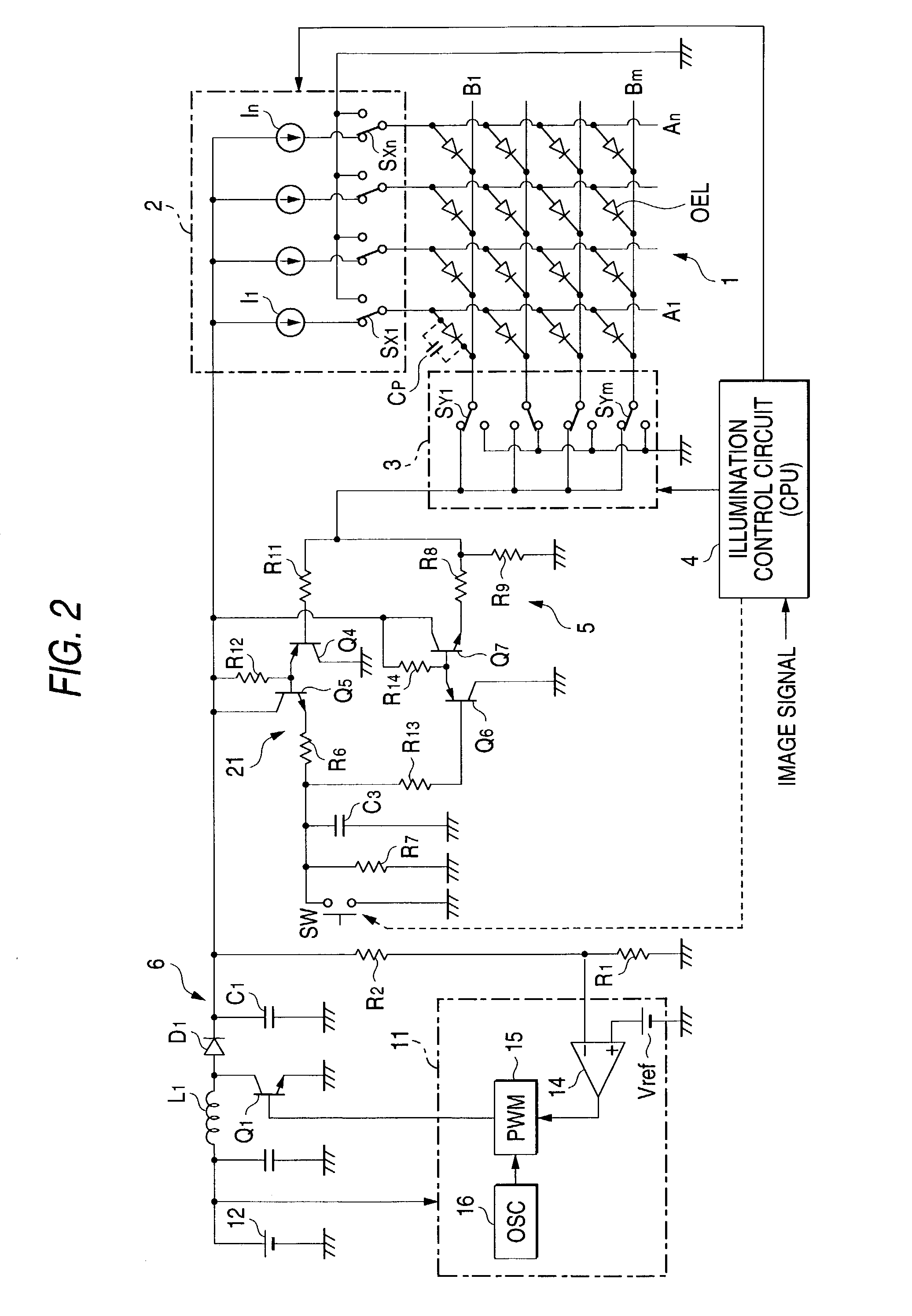
[0083]FIG. 3 shows the driving apparatus according to the invention. The apparatus shown in FIG. 3 is identical in principal configuration with that shown in FIG. 2, and corresponding elements are assigned the same reference numerals. Hence, their detailed explanations are omitted. In the embodiment shown in FIG. 3, a boosted output from a DC-DC converter is controlled by utilization of a voltage appearing in the terminal of the capacitor C3 held by the peak holding circuit 2, thereby diminishing power loss associated with driving of the display panel 1.

[0084]In the embodiment shown in FIGS. 1 and 2, an output from the DC-DC converter 6 to be applied to the respective constant current circuits I1 through In in the anode line drive circuit 2 is controlled so as to become a substantially-constant output voltage (constant voltage) at all times, by means of, e.g., a switching regulator utilizing the PWM system. In this case, there is no alternative but to set the voltage output from the...


PUM


Abstract

In an apparatus for driving a luminescent display panel, in a state in which scanning lines are sequentially scanned to drive and illuminate light-emitting elements, a voltage peak value arising in a scanning line in a non-scanning state is held by a capacitor through parasitic capacitance of the light-emitting element in a non-scanning state. On the basis of the voltage value held by the capacitor, a reverse bias voltage to be output from a reverse bias voltage generation circuit is controlled, and the voltage is supplied to the scanning lines.

Description

BACKGROUND OF THE INVENTION[0001]1. Field of the Invention[0002]The present invention relates to a technique for driving a capacitive light-emitting element; e.g., an organic electroluminescence (EL) element, to emit light. Particularly, the invention relates to an apparatus and method for driving a luminescent display panel which suppresses occurrence of crosstalk illumination of EL elements and can offer a suitable luminous brightness characteristic by means of appropriately controlling a reverse bias voltage to be applied to cathode scanning lines in a non-luminous state, as required, when a display panel having a plurality of organic EL elements arranged thereon is driven.[0003]2. Description of the Related Art[0004]An organic EL display has already been put into actual use in some quarters as a display which serves as an alternative to a liquid-crystal display and enables realization of low power consumption, high display quality, and a lower profile. An underlying backdrop to ...

Claims


Application Information

Patent Timeline
IPC IPC(8): G09G3/30G09G3/10G09G5/00G09G5/10H01L51/50G09G3/20G09G3/32
CPCG09G3/3216G09G3/3266G09G3/3283G09G2310/0256G09G2320/029G09G2320/041G09G2320/043G09G2330/02
Inventor YAZAWA, NAOKIHENMI, KOJISUZUKI, GENMORIYA, KEISUKEOKUYAMA, TAKESHI
Owner TOHOKU PIONEER CORP
Why Eureka
Try Eureka