
Reduced turn-on current content addressable memory (CAM) device and method

a technology of content addressable memory and current draw, which is applied in the direction of digital storage, instruments, computing, etc., can solve the problems of large change in the current requirement of the device, the current draw of the cam device is particularly problematic, and the current draw of the cam device can be considerabl

Active Publication Date: 2006-08-29
AVAGO TECH INT SALES PTE LTD
View PDF12 Cites 8 Cited by
  • Summary
  • Abstract
  • Description
  • Claims
  • Application Information

AI Technical Summary

Benefits of technology

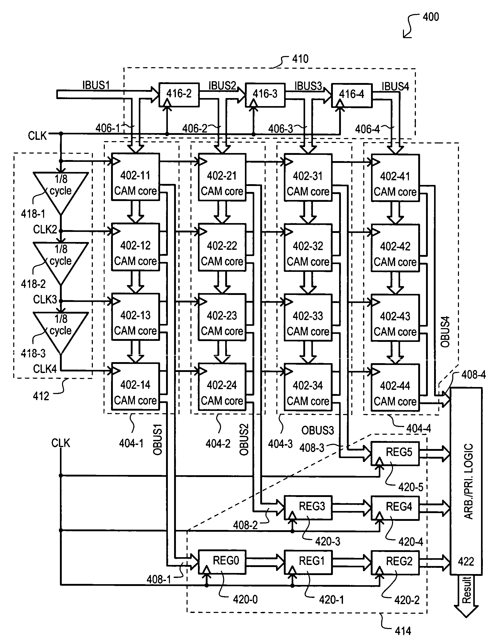
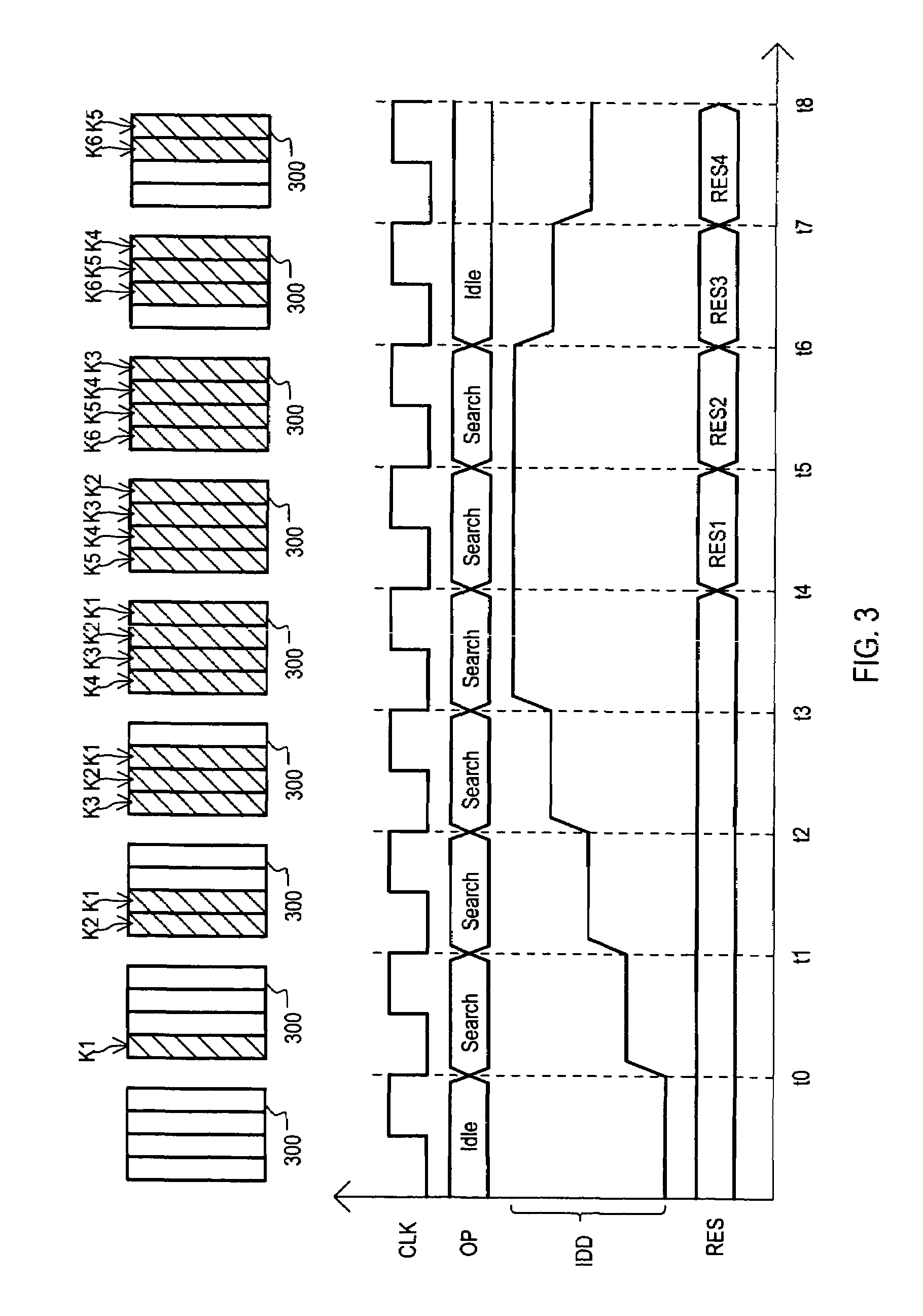
[0032]In such an arrangement, current drawn in a start-up operation can be gradually increased by sequential activation of different sections, as well sequential activation of blocks within each section. As a result, undesirably large current surges can be reduced or eliminated.
[0034]Such a feature provides peak current savings for CAM operations that typically draw the most current (searches).
[0039]In this way, command data (e.g., search commands and keys) can propagate from one section to the next according to a single clock signal. Such an arrangement can ensure that processing throughput is maintained, while introducing some latency into the results.
[0041]Such an arrangement can provide a compact way of generating sequential activation signals for blocks within each section.
[0045]Such an arrangement spaces the activation of blocks in time to help ensure that power supplies and or inherent parasitic elements have sufficient time to recover from resulting current surges.
[0049]Such an arrangement can enable sequentially generated search results from multiple sections to be synchronized for common application to a result logic circuit according to one common clock signal.

Problems solved by technology

As a result, CAM devices can draw considerable current as match lines in the CAM cell array are continuously charged and discharged each clock cycle.
Current draw in CAM device can be particularly problematic in the case of a “cold start” operation.
When CAM device portions (i.e., cores or blocks) go from an idle to an active state, there can be a very large change in the current requirement for the device.
In current generation parts, such a current surge can be too large for the on-chip capacitance to support and can happen too quickly for capacitors to respond on circuit boards associated with the CAM device.
Still further, parasitic inductance of a package containing a CAM device, as well as inductance inherent in a CAM device mounting arrangement can prevent a fast ramp up of the current, preventing an adequate current supply when needed by the CAM device.
The above deficiencies can result in a power supply voltage “sag” (i.e., level dip) within the CAM device.
In addition, the rapid change in current (dl / dt) through parasitic inductive elements can give rise to ground “bounce” (transient jump in a low supply voltage level), which can further disturb CAM operations.
These undesirable variations in supply voltages can lead to failures.
Such an arrangement can help to spread out current demand within a cycle, however, as CAM devices increase in capacity and operating speed, such an approach may not be sufficient to eliminate cold start and related problems.
This limit represents a current surge value at which errors can occur and / or device reliability can be compromised.
The above noted current surges can cause supply dips, which in turn, can cause device failures.
It is believed that the above-described errors are most likely to occur in the case of a single bit miss, where a single exclusive-OR (XOR) stack within one CAM cell of an entry has to discharge an entire match line.
Increases in supply current surges, like those noted above, can result in other drawbacks.
Such rises in the supply voltages can stress the gate oxide of metal-oxide-semiconductor (MOS) type transistors, increasing the possibility of oxide breakdown in such devices.
In addition, such increases in supply level can lead to electromigration in conductive lines, which can lead to higher resistance signal lines, or in a worst case, opens.

Method used


Image

  • Reduced turn-on current content addressable memory (CAM) device and method
  • Reduced turn-on current content addressable memory (CAM) device and method
  • Reduced turn-on current content addressable memory (CAM) device and method

Examples


first embodiment

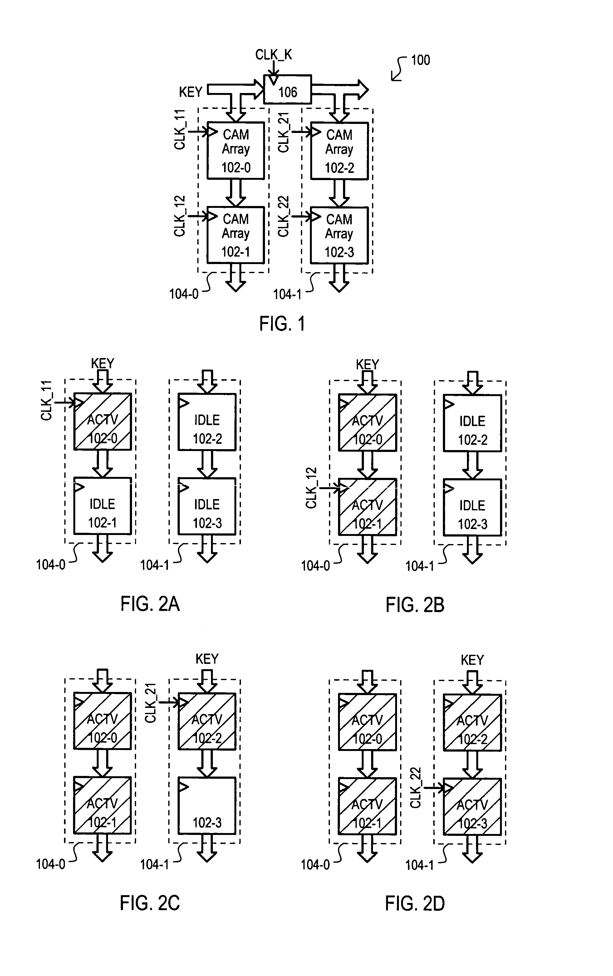
[0069]A CAM device is shown in FIG. 1, and designated by the general reference character 100. A CAM device 100 can include a number of CAM arrays 102-0 to 102-3. It is understood that each CAM array (102-0 to 102-3) can include a number of CAM entries, each of which can compare a key value KEY to a stored data value and generate a match result as a response.

[0070]The CAM arrays (102-0 to 102-3) can be conceptualized as being arranged into a 2×2 matrix, with two rows and two columns. Columns can be conceptualized as being sections 104-0 and 104-1. In a search operation, each section (104-0 and 104-1) can receive a search key value KEY in a sequential fashion. That is, a search KEY can be applied to first section 104-0, and a predetermined time later, can be applied to a next section 104-1.

[0071]In the very particular example of FIG. 1, sequential application of a search key value is accomplished by a register 106 controlled by a clock signal CLK_K.

[0072]In this way, a CAM device can...

third embodiment

[0092]A CAM device is shown in a detailed block schematic diagram in FIG. 4, and designated by the general reference character 400. A CAM device 400 can include a number of CAM “cores”402-11 to 402-44. Each CAM core (402-11 to 402-44) can include a number of CAM entries that a search operation can compare stored data with an applied search key and provide search results. Thus, in some embodiments a CAM core can include prioritizing and encoding circuits.

[0093]CAM cores (402-11 to 402-44) can be organized into a number of sections 404-1 to 404-4. Each section (404-1 to 404-4) can receive a command and key data by way of a corresponding input bus 406-1 to 406-4. Command and key data received by a section (404-1 to 404-4) can be applied in parallel or sequentially to the corresponding CAM cores of the section. In response to command and key data, each section (404-1 to 404-4) can provide result data on a corresponding output bus 408-1 to 408-4. More particularly, a CAM core (402-11 to...


PUM


Abstract

A content addressable memory (CAM) device (400) can sequentially apply command and key data to different sections (404-1 to 404-4). Within each section, CAM cores (402-11 to 402-44) can be sequentially activated. Current surges when transitioning from an idle state to an active state, or vice versa, can be significantly reduced with additional latency but no loss in throughput.

Description

TECHNICAL FIELD[0001]The present invention relates generally to content addressable memory (CAM) devices, and more particularly to the execution of operations, such as search operations, within CAM devices.BACKGROUND OF THE INVENTION[0002]Content addressable memory (CAM) devices, sometimes also referred to as “associative memories”, can provide rapid matching functions between an applied data value (e.g., a comparand, compare data, or search key) and stored data values (e.g., entries). Such rapid matching functions are often utilized in routers, network switches, and the like, to process network packets.[0003]A typical CAM device can store a number of data values in a CAM cell array. In a compare (i.e., search) operation, entries can be compared to a compare data value (i.e., key). An entry that matches the key can result in the generation of a match indication.[0004]In a conventional CAM device, search operations can be conducted in response to a system clock, with searches being u...

Claims


Application Information

Patent Timeline
IPC IPC(8): G11C15/00
CPCG11C15/00
Inventor NARUM, STEVENOM, HARIMASRI, NABIL M.
Owner AVAGO TECH INT SALES PTE LTD
Learn More