Semiconductor module having heat sink serving as wiring line
a technology of semiconductor modules and heat sinks, applied in the direction of semiconductor devices, semiconductor/solid-state device details, electrical apparatus, etc., can solve problems such as failure to supply the required voltage to circuitry, operation errors or malfunctions, and voltage drop-down
- Summary
- Abstract
- Description
- Claims
- Application Information
AI Technical Summary
Benefits of technology
Problems solved by technology
Method used
Image
Examples
first embodiment
[0028][First Embodiment]
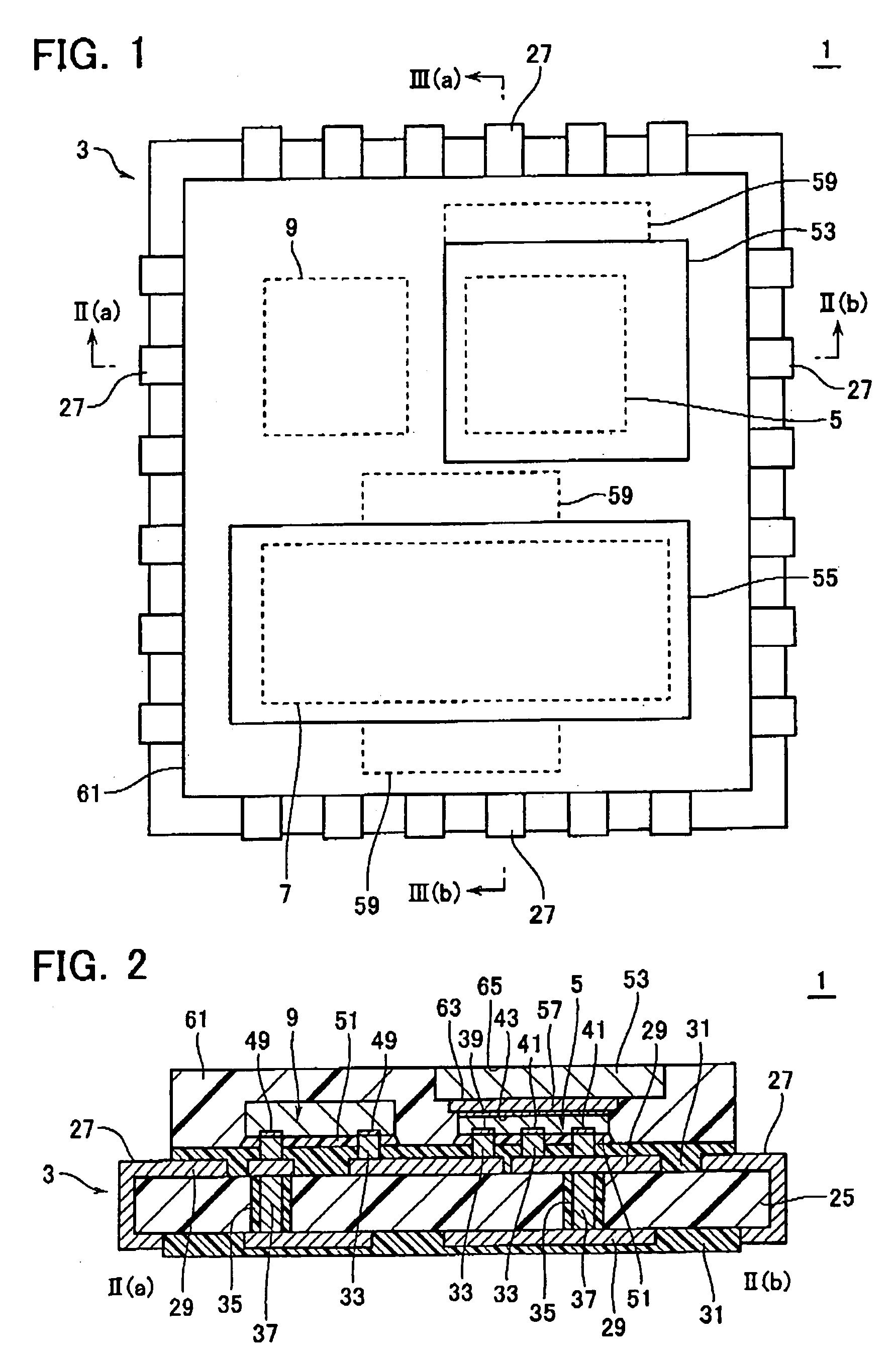
[0029]The structure of a semiconductor module in accordance with a first embodiment of the invention will be explained with reference to FIGS. 1 to 3. FIG. 1 is a plan view of the semiconductor module in accordance with the first embodiment. FIG. 2 is a cross-sectional diagram of the module as taken along line II(a)–II(b) of FIG. 1, whereas FIG. 3 is a sectional view taken along line III(a)–III(b) of FIG. 1.
[0030]The semiconductor module 1 has a parts-mounting or packaging substrate (for example, printed wiring board) 3 and IC chips mounted thereon, wherein the chips include two power MOS chips 5 and 7 and an IC chip 9 for drive use. The driver IC chip 9 is for driving the gates of MOSFETs formed on the power MOS chips 5 and 7.
[0031]FIG. 4 shows a sectional view of part of the power MOS chip 5, 7. The chip 5, 7 is structured so that a great number of vertical type MOSFETs are connected in parallel with one another. Explaining in more detail, the chip 5, 7 has...
second embodiment
[0063][Second Embodiment]
[0064]FIG. 8 is a diagram showing a plan view of a semiconductor module 81 in accordance with a second embodiment of the invention. FIG. 9 is a cross-sectional diagram of the module of FIG. 8 as taken along line IX(a)–IX(b). The second embodiment will be set forth with reference to FIGS. 8–9 while focusing an explanation on its differences from the first embodiment.
[0065]In the second embodiment, the heat sink 53 that covers the power MOS chip 5 extends to overlie the driver IC chip 9, thereby covering the driver IC chip 9. This permits the power MOS chip 5 and the driver IC chip 9 to commonly use or “share” the heat sink 53. Accordingly, the heat sink is allowed to have a larger area when compared to the case where a separate heat sink covering the driver IC chip 9 is laid out in addition to the heat sink 53. This makes it possible to improve the heat releasability by a degree corresponding thereto.
[0066]Note however that the back face 83 of driver IC chip ...
third embodiment
[0070][Third Embodiment]
[0071]A third embodiment is different from the embodiments stated above in that the former is equipped with a power MOS chip (synchronous rectification-side element) 7 with a built-in SBD 69. FIG. 10 illustrates, in cross-section, part of the power MOS chip (synchronous rectification-side element) 7 equipped in the third embodiment, which corresponds to FIG. 4. The SBD 69 is formed so that it is spaced apart by a specified distance from a terminate end 85 of a MOSFET fabrication region. This specified distance is a distance which avoids any appreciable interference between the MOSFET and SBD.
[0072]The SBD 69 is configured from an epitaxial layer 11 and a metallic film 87 made of aluminum or the like, which is formed thereon. The epitaxial layer 11 and metal film 87 are contacted together, resulting in formation of a Schottky barrier at such contact portion. SBD 69 is connected in parallel to the MOSFET of power MOS chip 7. The SBD 69 may be replaced with a pn...
PUM
 Abstract
Description
Claims
Application Information
 - R&D
- Intellectual Property
- Life Sciences
- Materials
- Tech Scout
- Unparalleled Data Quality
- Higher Quality Content
- 60% Fewer Hallucinations
Browse by: Latest US Patents, China's latest patents, Technical Efficacy Thesaurus, Application Domain, Technology Topic, Popular Technical Reports.
© 2025 PatSnap. All rights reserved.Legal|Privacy policy|Modern Slavery Act Transparency Statement|Sitemap|About US| Contact US: help@patsnap.com


