
Multilayer printed wiring board having filled-via structure

a printing board and via hole technology, applied in the direction of printed element electric connection formation, insulating substrate metal adhesion improvement, dielectric characteristics, etc., can solve the problems of metal deposit likely to break, surface portion of plating metal exposed outside the hole for via hole, etc., to achieve improved adhesion between the via hole and interlaminar insulative resin layer, the effect of not easily broken and larger malleability

Inactive Publication Date: 2006-07-04
IBIDEN CO LTD
View PDF42 Cites 53 Cited by
  • Summary
  • Abstract
  • Description
  • Claims
  • Application Information

AI Technical Summary

Benefits of technology

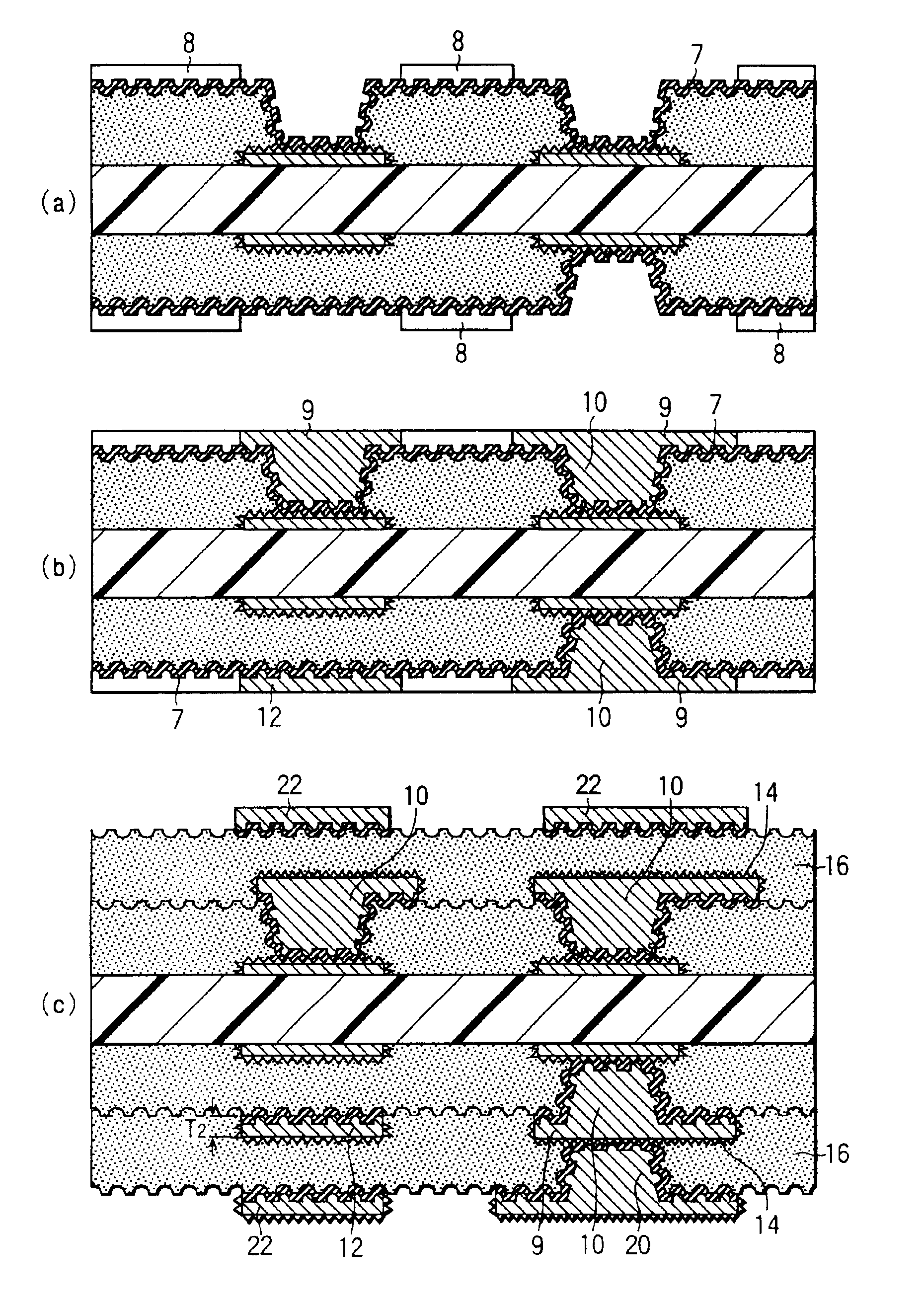
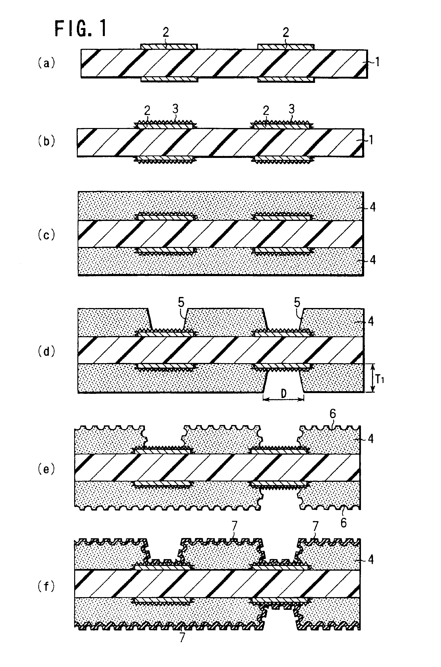
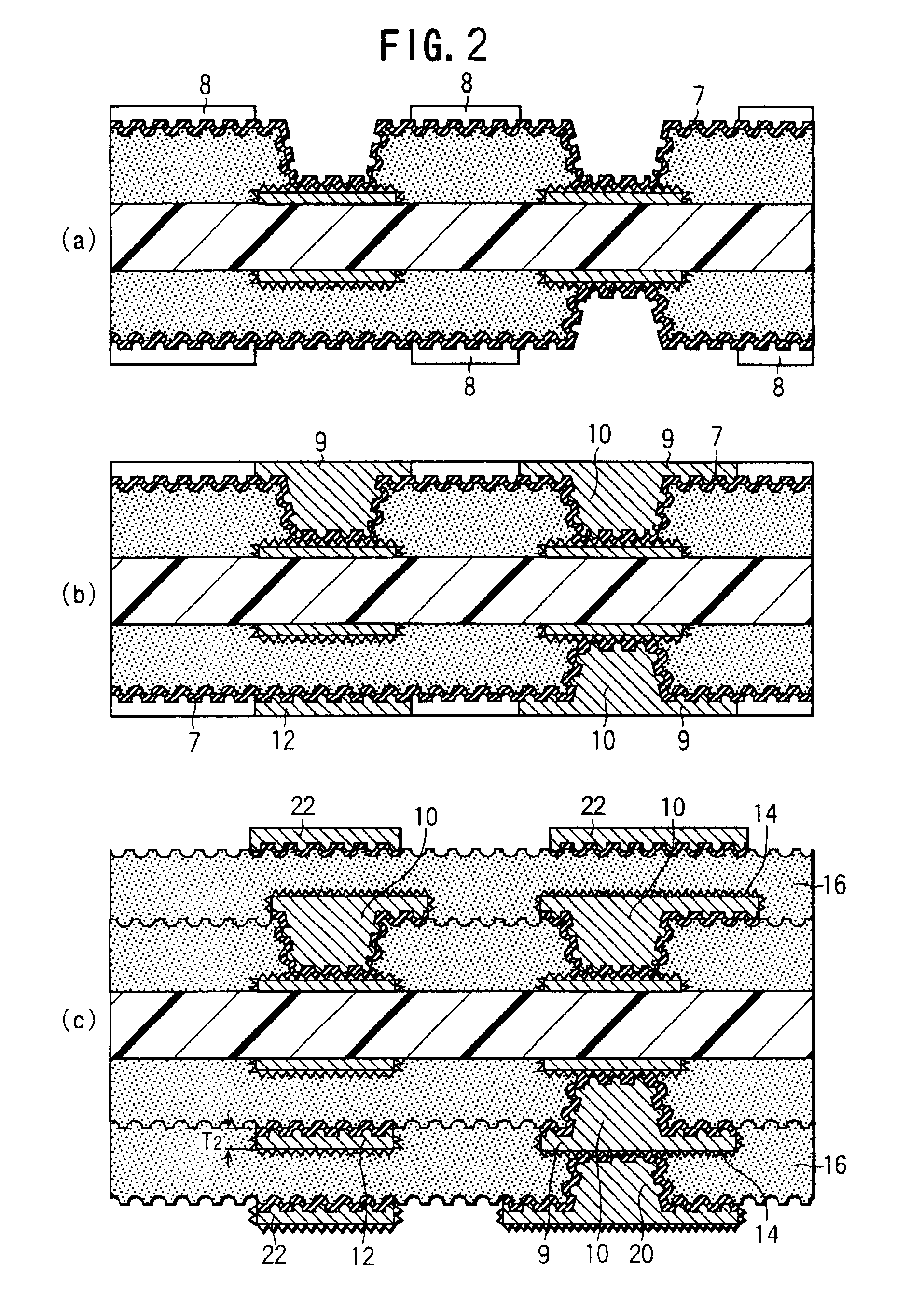
The present invention provides a multilayer printed wiring board with secure adhesion between the various layers and improved reliability of the electrical connection. This is achieved by roughening the surfaces of the interlaminar insulative resin layers and the conductor circuitry layer to enhance adhesion, and by using a composite of thermoplastic resin and thermosetting resin or only thermosetting resin to fill the viaholes. The ratio between the viahole diameter and the interlaminar insulative resin layer should be within a range of 1 to 4 for finer patterning. The thickness of the conductor circuitry layer should be less than ½ of the viahole diameter and less than 25 μm for easier formation of a fine pattern.

Problems solved by technology

However, the multilayer printed wiring board having such viaholes formed through them are not advantageous in that the metal deposit is likely to break due to its precipitation or a heat cycle.
The multilayer printed wiring board having the filled viahole structure is however disadvantageous in that a surface portion of the plating metal exposed outside the hole for viahole (the surface will be referred to as “viahole surface” henceforth) is easily depressible.
If an interlaminar insulating layer resin is formed on a conductor circuitry layer irrespectively of such a depression existent on the viahole surface, a corresponding depression will develop on the surface of the interlaminar insulative resin layer, and cause the plating metal film to break and also a trouble in mounting electronic parts on the wiring board.
Especially for mass production of multilayer printed wiring boards, the residual resin is likely to occur since it is difficult to set different exposure and development conditions for the viahole surface from those for the conductor circuitry layer surface.
Furthermore, since in the filled viahole structure, a plating metal is filled in a hole for viahole, a larger stress will be caused by heat cycle than in a viahole formed just by plating an inner wall and bottom of a hole, so that a crack is likely to occur first in the viahole and then spread to an interlaminar insulative resin layer.
However, the plating layer applied by the electroless plating is harder and less malleable than a one applied by the electroplating.
Therefore, the plating layer is likely to crack under a thermal shock or due to heat cycle.

Method used


Image

  • Multilayer printed wiring board having filled-via structure
  • Multilayer printed wiring board having filled-via structure
  • Multilayer printed wiring board having filled-via structure

Examples


example 1

[0170](1) Compositions prepared through the following steps ① to ② were mixed together and agitated to prepare an electroless plating adhesive.[0171]① Thirty-five parts by weight of a 25% acrylated product of cresol novolac type epoxy resin (80% in sold content; 250 in molecular weight, by Nippon Kayaku Co., Ltd.), 4 parts by weight of photosensitive monomer (ARONIX M315 by Toa Gosei Co., Ltd.), 0.5 part by weight of antifoaming agent (S-65 by SANNOPCO) and 3.6 parts by weight of NMP, were mixed by agitation.[0172]② Eight parts by weight of polyether sulfone (PES) and 7.245 parts by weight of epoxy resin particles (POLYMERPOE by Sanyo Kasei Co., Ltd.) of 0.5 μm in mean particle size were mixed together and then 20 parts by weight of NMP were added to the mixture. They were mixed by agitation.[0173]③ Two parts by weight of imidazole curing agent (2E4MZ-CN by Shikoku Kasei Co., Ltd.), 2 parts by weight of initiator (IRGACURE I-907 by Ciba Geigy), 0.2 part by weight of photosensitizer ...

example 2

[0187]A multilayer printed wiring board was prepared in the same manner as the aforementioned example 1 except that an interlaminar insulative resin layer was formed by attaching a fluororesin film of 20 μm in thickness to the layer by thermo-compression bonding and holes for viaholes of 60 μm in diameter were formed by irradiating ultraviolet laser.

example 3

[0188](1) A drawn tetrafluoroethylene resin (PTFE) fiber available as fiber for woven fabric from the W. L. Gore & Associates, Inc. (trade name: GORE-TEX) was used to weave a cloth for an interlaminar insulative resin layer. The cloth was composed of 53 fibers of 400 deniers per 2.54 cm in longitudinal direction and 52 fibers of 400 deniers per 2.54 cm in lateral direction.

[0189](2) The fluororesin fiber cloth was cut to a sheet of 15.24 cm by 15.24 cm, and the cloth sheet was immersed in a solution of alkaline metal and naphthalene available under the trade name TETRA-ETCH from the W. L. Gore & Associates. After that, the cloth sheet was washed in warm water to rinse away the acetone. The fibers appeared dark brown due to the etching and the cloth shrank 20% in both longitudinal and lateral directions. The cloth sheet was stretched to the initial dimensions with the edges thereof held in hands.

[0190]On the other hand, a liquid epoxy resin was prepared as a thermosetting resin which...


PUM

PropertyMeasurementUnit
depthaaaaaaaaaa
thicknessaaaaaaaaaa
diameteraaaaaaaaaa

Abstract

The present invention provides a multilayer printed wiring board having a filled viahole structure advantageously usable for forming a fine circuit pattern thereon, and having an excellent resistance against cracking under a thermal shock or due to heat cycle. The multilayer printed wiring board is comprised of conductor circuitry layers and interlaminar insulative resin layers deposited alternately one on another, the interlaminar insulative resin layers each having formed through them holes each filled with a plating layer to form a viahole. The surface of the plating layer exposed out of the hole for the viahole is formed substantially flat and lies at a substantially same level as the surface of the conductor circuit disposed in the interlaminar insulative resin layer. The thickness of the conductor circuitry layer is less than a half of the viahole diameter and less than 25 μm. The inner wall of the hole formed in the interlaminar insulative resin layer is roughened and an electroless plating layer is deposited on the roughened surface. An electroplating layer is filled in the hole including the electroless plating layer to form the viahole. The interlaminar insulative resin layer is formed from a composite of a fluororesin showing a high fracture toughness and a heat-resistant thermoplastic resin, a composite of fluororesin and thermosetting resin or a composite of thermosetting and thermoplastic resins.

Description

BACKGROUND OF THE INVENTION[0001]1. Field of the Invention[0002]The present invention relates to a multilayer printed wiring board having a filled viahole structure, and more particularly to a multilayer printed wiring board adapted to assure an outstandingly secure adhesion between a conductor circuitry layer and an interlaminar insulative resin layer and form a fine conductor circuit pattern.[0003]2. Description of Background Information[0004]The multilayer printed wiring board includes a build-up multilayer printed wiring board in which conductor circuitry layers and insulative resin layers are alternately formed one on another and inner and outer ones of the conductor circuitry layers are electrically connected to each other by viaholes formed in the insulative resin layers. Generally, the viaholes in such a multilayer printed wiring board are formed by depositing a plating metal film on the inner wall and bottom of each of fine holes formed through the interlaminar insulative r...

Claims


Application Information

Patent Timeline
Patent Type & Authority Patents(United States)
IPC IPC(8): H05K1/11H01R12/04H05K3/10H05K3/38H05K3/42H05K3/46
CPCH05K3/421H05K3/4661H05K3/108Y10T428/24322H05K3/382H05K3/423H05K2201/0129H05K2201/015H05K2201/0278H05K2201/09563H05K2201/096H05K2201/09745Y10T428/24273Y10T428/24917H05K3/381Y10T428/31681H05K3/46
Inventor SHIRAI, SEIJISHIMADA, KENICHIASAI, MOTOO
Owner IBIDEN CO LTD
Learn More