
Magnetoresistive element, magnetic memory cell, and magnetic memory device

a technology of magnetic memory cell and magnetic memory device, which is applied in the direction of digital storage, semiconductor devices, instruments, etc., can solve the problems of difficult to perform sufficiently stable writing operation, and achieve the effect of stably writing by efficiently using

Inactive Publication Date: 2006-06-20
TDK CORPARATION
View PDF17 Cites 11 Cited by
  • Summary
  • Abstract
  • Description
  • Claims
  • Application Information

AI Technical Summary

Benefits of technology

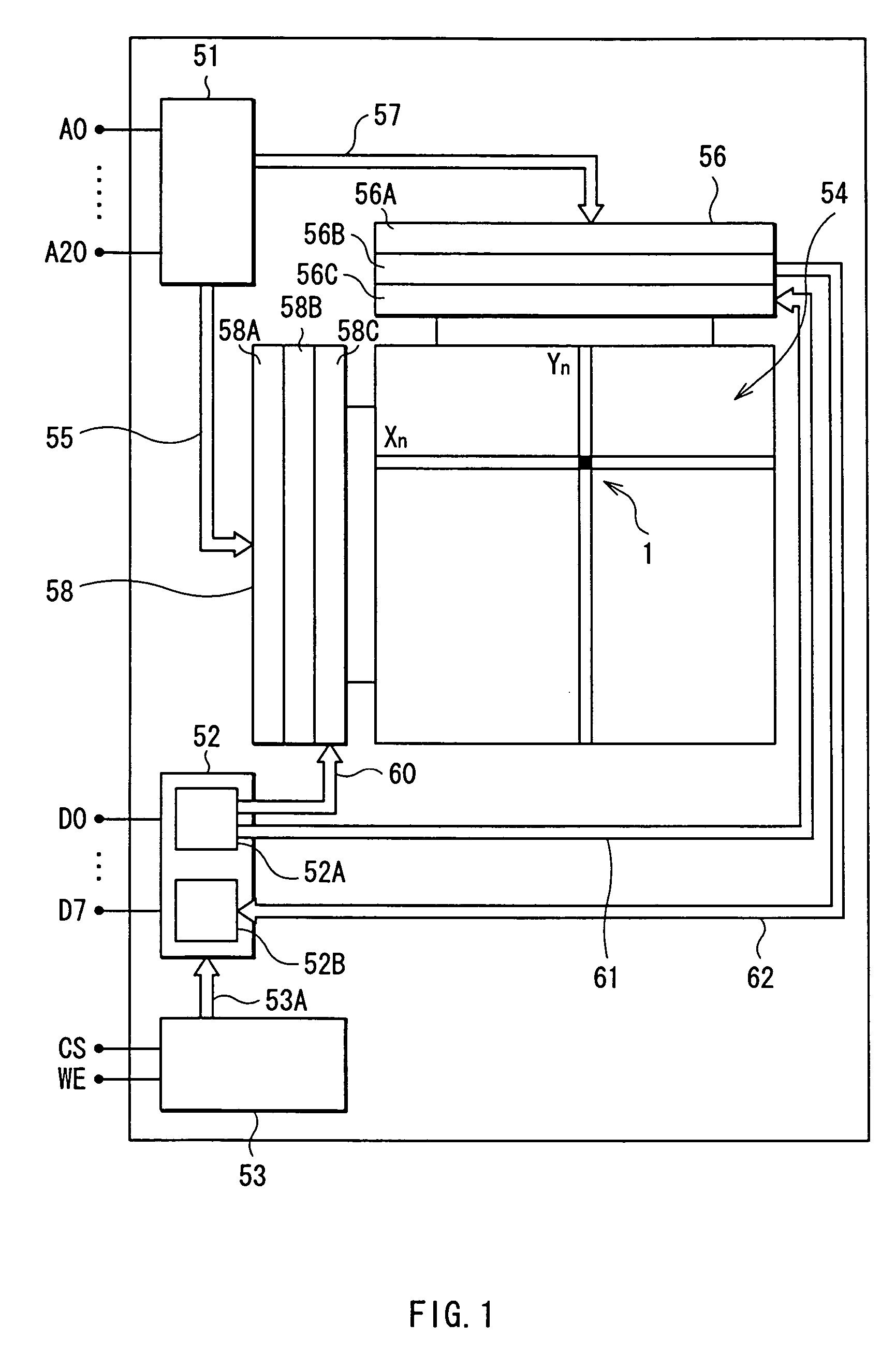
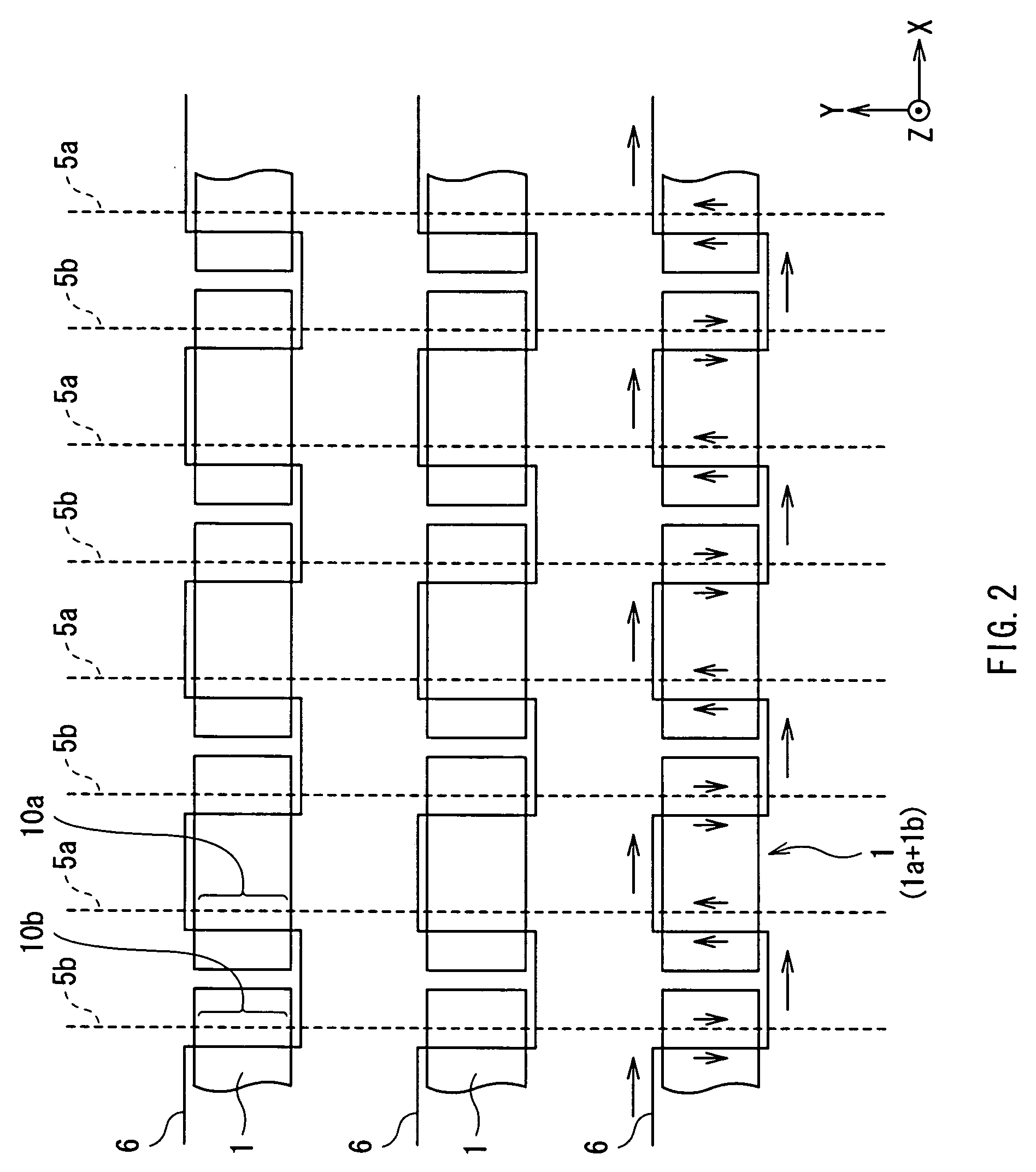
The present invention provides a magneto-resistive element, a magnetic memory cell, and a magnetic memory device that can efficiently write information using a magnetic field generated by current flowing in a conductor. The magneto-resistive element includes a magnetic yoke and a stacked body with a magneto-sensitive layer that changes its magnetization direction when an external magnetic field is applied. The area of a cross section perpendicular to the extension direction of the conductor is the smallest in the part connected to the stacked body. This results in the highest magnetic flux density in the connection part, allowing for efficient inversion of the magneto-sensitive layer with a smaller write current. The magnetic memory device includes a first write line and a second write line extending parallel to the first write line and constructed to cross it, and a magnetic memory cell with a magneto-resistive element. The area of a cross section perpendicular to the extension direction of the conductor is the smallest in the part connected to the stacked body.

Problems solved by technology

Consequently, it is expected that as the write current is being weakened, it becomes difficult to perform sufficiently stable writing operation.

Method used


Image

  • Magnetoresistive element, magnetic memory cell, and magnetic memory device
  • Magnetoresistive element, magnetic memory cell, and magnetic memory device
  • Magnetoresistive element, magnetic memory cell, and magnetic memory device

Examples


first modification

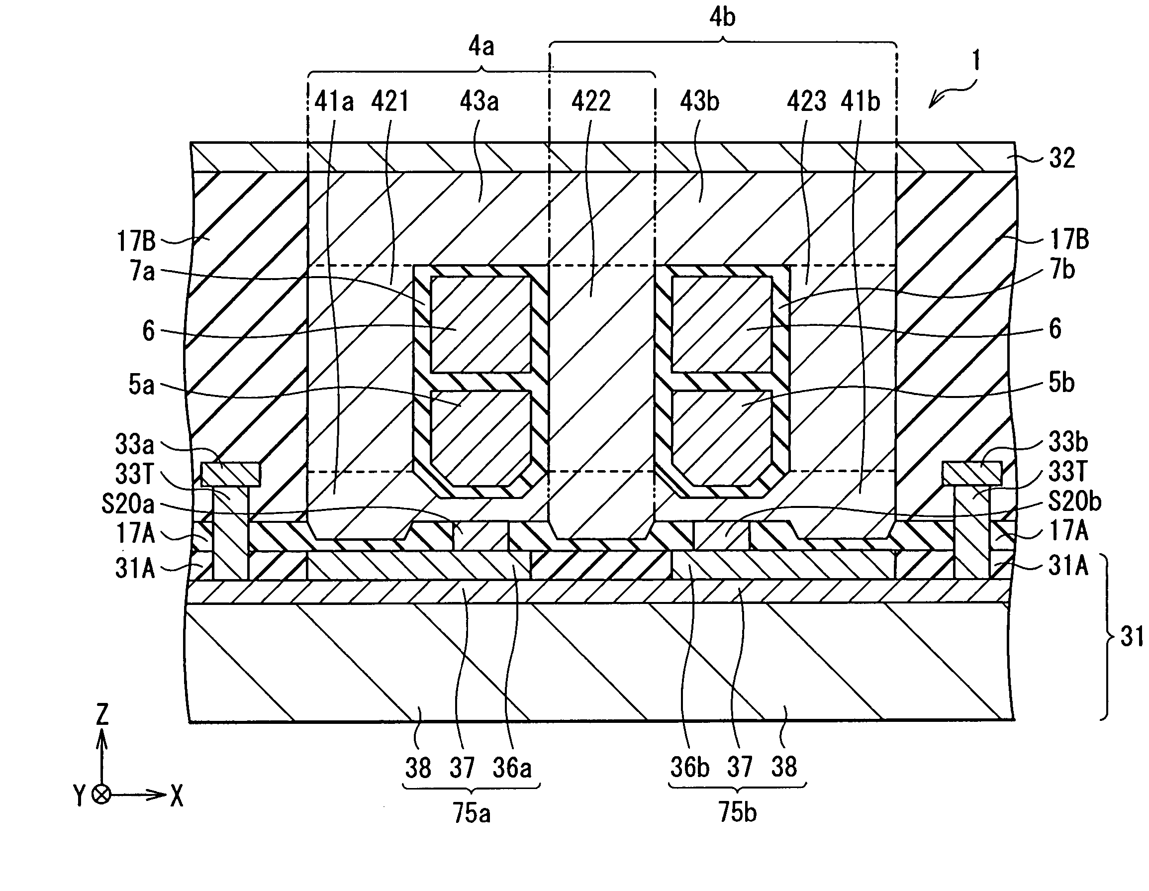
[0144]FIGS. 30A and 30B show the configuration of a memory cell 1V1 as a first modification of the embodiment. FIG. 30A shows the configuration of an XY plane parallel to the stacked face of the stacked bodies S20a and S20b. FIG. 30B is a cross section taken along line XXX(B)—XXX(B) of FIG. 30A. As described above, in the embodiment, the first beam yokes 41a and 41b in the magnetic yokes 4a and 4b are constructed so that the width in the extending direction (Y-direction) of the write bit lines 5a and 5b and the write word line 6 becomes the minimum in the connection parts 14a and 14b and the width of the stacking direction (Z direction) of the stacked bodies S20a and S20b in the connection parts 14a and 14b, that is, the thickness becomes the minimum in the connection parts 14a and 14b. In contrast, in the memory cell 1V1 of the modification, the magnetic yoke 4V1 is constructed so that the thickness of the first beam yoke 41 becomes uniform and width W14 in the Y-direction of the c...

second modification

[0145]FIGS. 31A and 31B show the configuration of a memory cell 1V2 as a second modification of the embodiment. FIG. 31A shows the configuration of an XY plane parallel to the stacked face of the stacked bodies S20a and S20b. FIG. 31B is a cross section taken along line XXXI(B)—XXXI(B) of FIG. 31A. In the memory cell 1V1 of the first modification, the thickness of the first beam yoke 41V1 is made uniform and the width in the Y-direction of the connection parts 14a and 14b is made narrower than the adjacent parts. It is also possible to make the width W1 in the Y-direction of a first beam yoke 41V2 uniform and make the thickness T14 of the connection parts 14a and 14b smaller than the adjacent parts. Concretely, the memory cell 1V2 is constructed to have thickness T41 larger than the thickness T14 of the connection parts 14a and 14b only by height T1 by making the first beam yoke 41V2 have the projection 41T projected toward the stacked bodies S20a and S20b only by the height T1.

third modification

[0146]FIGS. 32A and 32B show the configuration of a memory cell 1V3 as a third modification of the embodiment. FIG. 32A shows the configuration of an XY plane parallel to the stacked face of the stacked bodies S20a and S20b. FIG. 32B is a cross section taken along line XXXII(B)—XXXII(B) of FIG. 32A. In the memory cell 1V2 of the second modification, the projection 41T projected toward the stacked bodies S20a and S20b is provided. Alternately, like a memory cell 1V3 shown in FIGS. 32A and 32B, a first beam yoke 41V3 may have inclined faces 41AK on both sides of the connection parts 14a and 14b and the thickness increases to the side opposite to the stacked bodies S20a and S20b in the stacking direction (Z direction) of the stacked bodies S20a and S20b with distance from the connection parts 14a and 14b. Also in the configuration, the thickness T14 of the connection parts 14a and 14b can be made smaller than the thickness T41 of the portion adjacent to the connection parts 14a and 14b...


PUM


Abstract

The present invention provides a magneto-resistive element capable of stably performing information writing operation by efficiently using a magnetic field generated by current flowing in a conductor and to a magnetic memory device having the same. A magneto-resistive element is constructed so that the area of a cross section orthogonal to the circumferential direction of a pair of magnetic yokes becomes the smallest in connection parts facing stacked bodies. With the configuration, magnetic flux density of return magnetic fields generated by passing write current to write bit lines and write word lines can be made the highest in the connection parts. Thus, information can be written efficiently and stably.

Description

BACKGROUND OF THE INVENTION[0001]1. Field of the Invention[0002]The present invention relates to a magnetoresistive element and a magnetic memory cell each including a magneto-sensitive layer of which magnetization direction changes according to an external magnetic field, and to a magnetic memory device for recording / reading information by using a change in the magnetization direction of the magneto-sensitive layer in the magnetoresistive element and the magnetic memory cell.[0003]2. Description of the Related Art[0004]Conventionally, as general memories used for information processors such as a computer and a communication device, volatile memories such as a DRAM (Dynamic Random Access Memory) and an SRAM (Static RAM) are used. The volatile memories have to be refreshed by always supplying current to hold stored information. When the power source is turned off, all of information is lost, so that a nonvolatile memory as means for recording information has to be provided in additio...

Claims


Application Information

Patent Timeline
Patent Type & Authority Patents(United States)
IPC IPC(8): H01L29/76H01L27/105G11C11/16H01L21/8246H01L43/08
CPCG11C11/16G11C11/1675
Inventor HATATE, HITOSHIKAMIJIMA, AKIFUMI
Owner TDK CORPARATION
Learn More