
Fully digital transmitter including a digital band-pass sigma-delta modulator

a digital band-pass, fully digital technology, applied in the field of full duplex transceiver circuitry, can solve the problems of increasing complexity of the circuitry required for carrying out such high-frequency modulation and communication, reducing the cost of hardware, and relying to a large extent on analog transceiver circuitry. achieve the effect of low receive band nois

Active Publication Date: 2006-06-13
TEXAS INSTR INC
View PDF8 Cites 33 Cited by
  • Summary
  • Abstract
  • Description
  • Claims
  • Application Information

AI Technical Summary

Benefits of technology

This patent describes a fully digital architecture for a radio frequency (RF) transmitter that is suitable for use in low-voltage complementary metal-oxide-semiconductor (CMOS) technology. The architecture includes a digital upconverter mixer and a digital band-pass sigma-delta modulator that can control transmit noise leakage into nearby frequency bands. The architecture also includes digital filtering and power amplifier driver circuitry integrated with digital automatic gain control (AGC) circuitry. The technical effects of this invention include low receive band noise, asymmetrical noise cancellation, and high-band transmit frequencies. Additionally, the invention provides a digital band-pass sigma-delta modulator that can control transmit noise leakage into nearby frequency bands.

Problems solved by technology

The circuitry required for carrying out such high-frequency modulation and communication has become increasingly complex.
Despite this increasing complexity, there remains significant pressure to further reduce hardware cost.
However, conventional transceiver circuitry still relies to a large extent on analog circuitry, especially in transmitting and receiving radio frequency (RF) signals.
This analog circuitry and passive components such as inductors that are typically required in the analog domain, has limited the extent to which cost reduction and performance improvements, both in operational speed and also reduced power dissipation, can be attained.
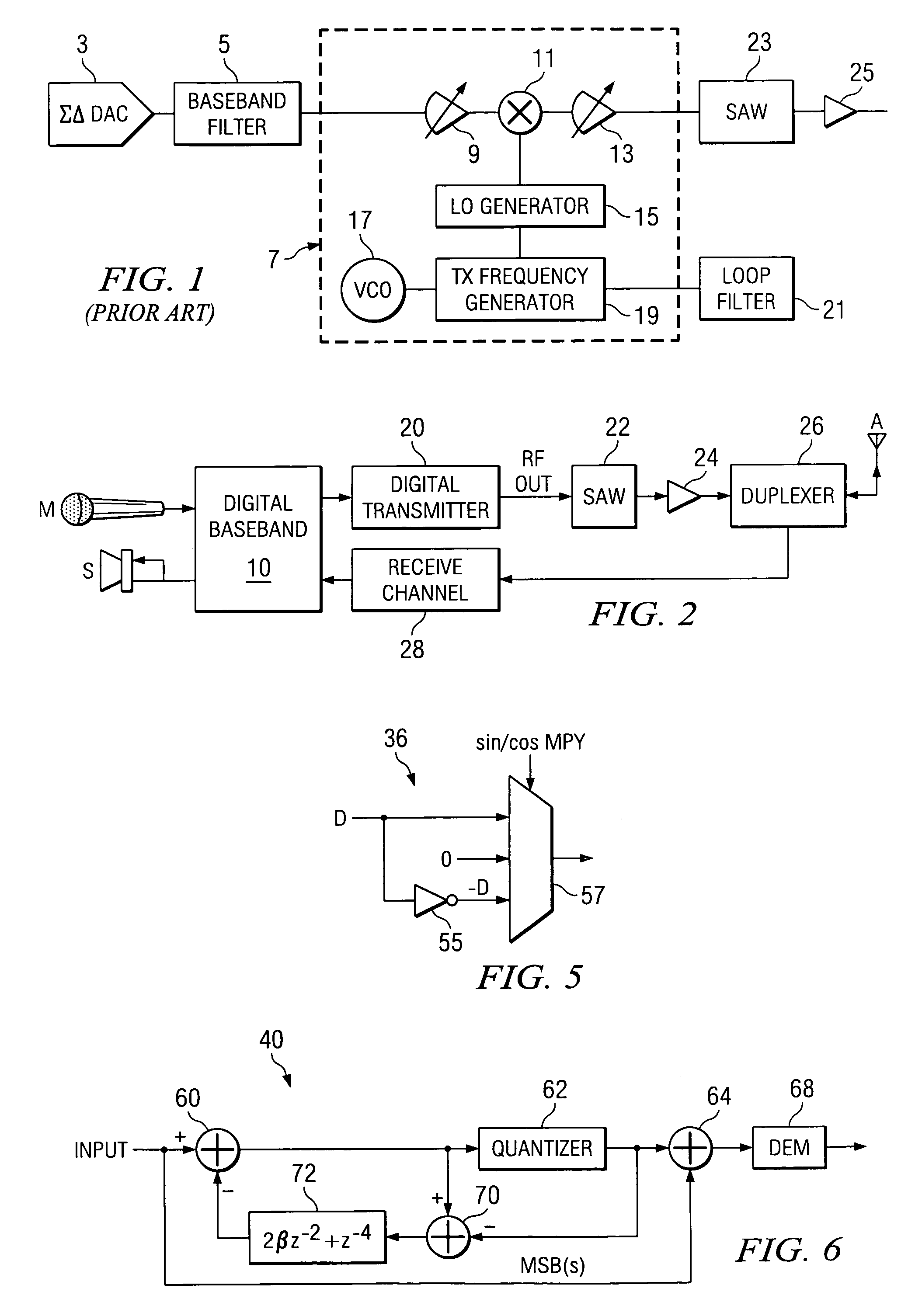
Analog AGC functions 9 and 13 in this conventional analog transmitter architecture also present issues both in realization and also in operation.
This AGC calibration typically involves significant test and characterization time in the manufacturing flow.
Indeed, the largest source of noise in the received signal at a conventional transceiver is typically the leakage from the signals that the transceiver is itself transmitting.
However, it has been observed that conventional analog transmitters cannot be constructed to have particularly low receive band noise, particularly if the manufacturing cost is to be kept reasonable (including using reasonable numbers of passive components).
Perhaps most importantly, the analog nature of much of the circuitry of the conventional transmitter of FIG. 1 makes it is difficult to highly integrate this transmitter into a single integrated circuit.
Further, as is well known in the art, analog circuitry cannot be readily realized by low-voltage complementary metal-oxide-semiconductor (CMOS) technology.
Rather, analog circuitry typically requires bipolar transistors, or at least a combination of bipolar and CMOS devices (e.g., BiCMOS technology), which is expensive from an integrated circuit manufacturing cost standpoint.
Bipolar transistors are not as readily scalable as CMOS devices, and as such it is contemplated that the integration efficiency that would be attained by CMOS integrated circuits in the future will not be available to analog circuits utilizing bipolar or BiCMOS technology.

Method used


Image

  • Fully digital transmitter including a digital band-pass sigma-delta modulator
  • Fully digital transmitter including a digital band-pass sigma-delta modulator
  • Fully digital transmitter including a digital band-pass sigma-delta modulator

Examples


Embodiment Construction

[0035]The present invention will be described in connection with its preferred embodiment, namely as implemented into a digital transceiver, such as may be used in connection with a wireless telephone handset, because it is contemplated that this application of the invention will especially benefit from its advantages. However, it is also contemplated that other applications of this invention can also benefit from its advantages. Accordingly, it is to be understood that the following description is provided by way of example only, and is not intended to limit the true scope of this invention as claimed.

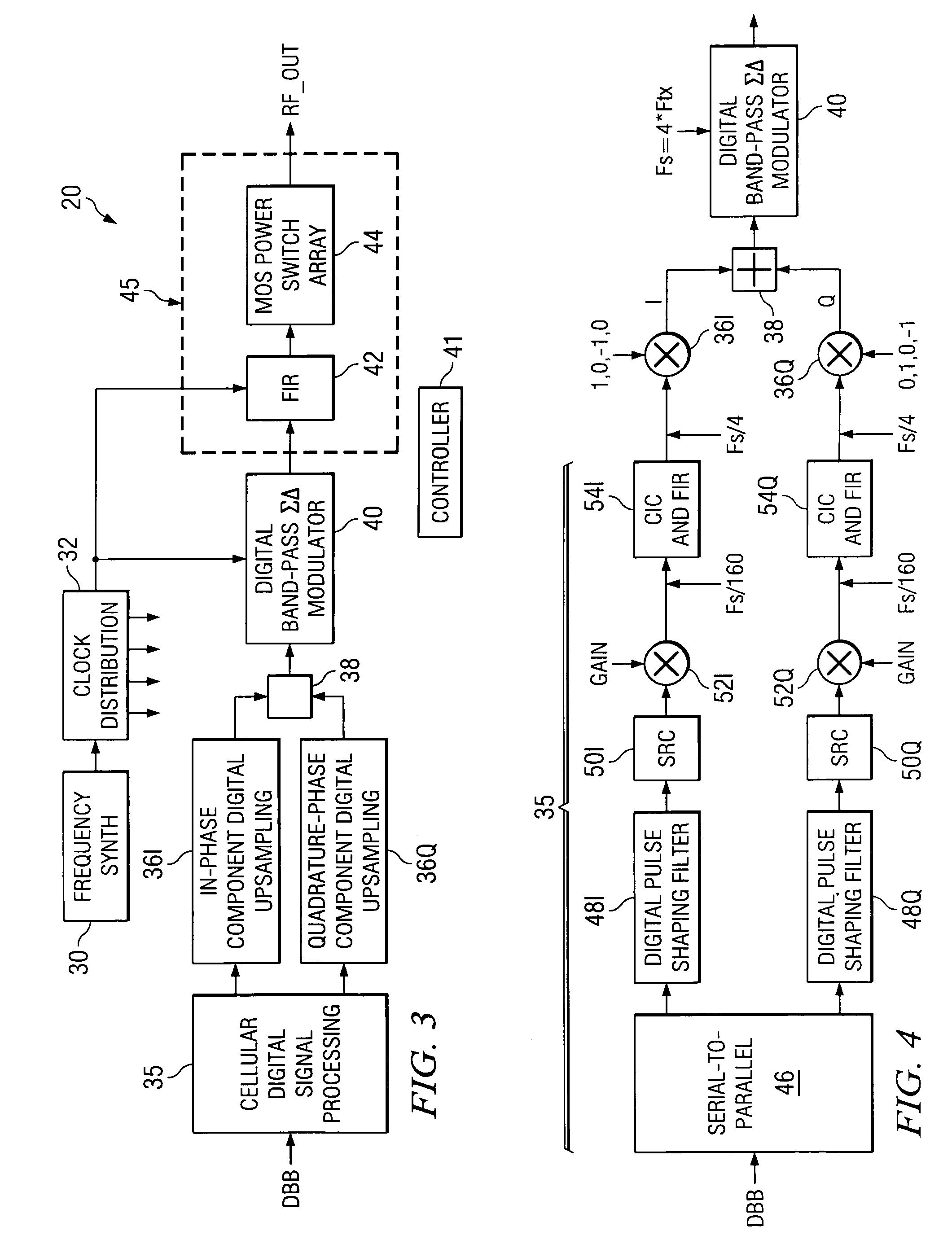
[0036]Referring first to FIG. 2, a communications system into which each of the preferred embodiments of this invention way be implemented will now be described. In the example of FIG. 2, the system is a wireless telephone handset, and as such includes microphone M coupled to provide signals to digital baseband processor 10 and then to digital transmitter 20, and speaker S that is cou...


PUM


Abstract

A digital transmitter (20) that may be advantageously used in a high-frequency transceiver, such as a wireless telephone handset, is disclosed. The transmitter (20) includes digital upconverter functions (36I, 36Q) that operate in combination with a digital band-pass sigma-delta modulator (40) to generate modulated digital signals at a sample frequency that is a multiple of the transmit frequency. The digital band-pass sigma-delta modulator (40) applies a noise transfer function in a feedback filter (72) in which the center of the pass band corresponds to the transmit frequency, and in which notches in the characteristic can be symmetrically or asymmetrically selected to correspond to specific frequencies, such as the receive band frequency, in which transmit noise is to be minimized. A combined FIR digital filter (42) and MOS power switch array (44) is also disclosed, in which a cascode arrangement of drain-extended MOS power transistors (78) and switching transistors (82) provide the output RF signal, with a coarse gain control (80) applied.

Description

CROSS-REFERENCE TO RELATED APPLICATIONS[0001]Not applicable.STATEMENT REGARDING FEDERALLY SPONSORED RESEARCH OR DEVELOPMENT[0002]Not applicable.BACKGROUND OF THE INVENTION[0003]This invention is in the field of transmitter and receiver circuitry, and is more specifically directed to full duplex transceiver circuitry such as used in modern mobile telephone handsets.[0004]Mobile telephone technology has greatly advanced in recent years, as evident by the higher performance digital mobile telephones now available. To a large extent, these advances stem from the widespread deployment of modern digital wireless modulation technologies such as time division multiple access (TDMA), code division multiple access (CDMA) technologies including conventional CDMA, wideband CDMA (WCDMA), and CDMA2000 standards, and personal communications service (PCS) modulation. The carrier frequencies for these modulated signals ranges from on the order of 800 MHz to as high as 2.0 GHz. These and other digita...

Claims


Application Information

Patent Timeline
Patent Type & Authority Patents(United States)
IPC IPC(8): H04L27/04H04L27/12H04L27/20H03F1/06H03F1/22
CPCH03F1/0205H03F1/223H04L27/20H04B1/0475H03F2200/331
Inventor BELLAOUAR, ABDELLATIFFONTAINE, PAUL-AYMERIC
Owner TEXAS INSTR INC
Learn More