
Gas chemistry cycling to achieve high aspect ratio gapfill with HDP-CVD

a gas chemistry and gap filling technology, applied in the field of integrated circuit manufacturing, can solve the problems of not being able to completely fill the gap, affecting device operation, and too prone to limitations when required to completely fill the high-aspect-ratio small-width gap

Inactive Publication Date: 2006-05-30
APPLIED MATERIALS INC
View PDF82 Cites 13 Cited by
  • Summary
  • Abstract
  • Description
  • Claims
  • Application Information

AI Technical Summary

Problems solved by technology

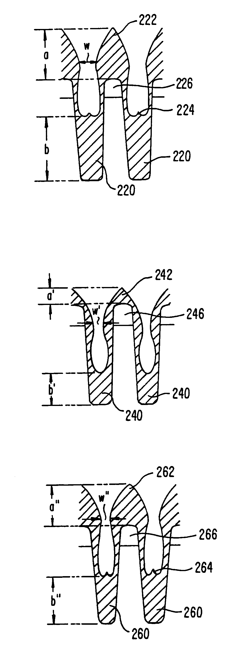
Gaps having a combination of a high aspect ratio and a small width present a challenge for semiconductor manufacturers to fill completely.
In short, the challenge usually is to prevent the deposited film from growing in a manner that closes off the gap before it is filled.
Failure to fill the gap completely results in the formation of voids in the deposited layer, which may adversely affect device operation, for example by trapping undesirable impurities.
While a TEOS-based chemistry does indeed have improved gapfill capabilities, it too runs up against limitations when required to completely fill sufficiently high-aspect-ratio small-width gaps.
HDP-CVD processes were not expected to share the same gapfill problems as other CVD processes.
It has been found in practice, however, that while HDP-CVD processes generally have better gapfill capabilities than similar non-HDP-CVD processes, for certain gap widths there remains a limit to the aspect ratio of gaps that can be filled.

Method used


Image

  • Gas chemistry cycling to achieve high aspect ratio gapfill with HDP-CVD
  • Gas chemistry cycling to achieve high aspect ratio gapfill with HDP-CVD
  • Gas chemistry cycling to achieve high aspect ratio gapfill with HDP-CVD

Examples


Embodiment Construction

I. Introduction

[0022]Embodiments of the present invention are directed to a method and apparatus for depositing a dielectric film on a substrate. For gaps with a given width, these embodiments using gas chemistry cycling within an HDP-CVD environment permit the dielectric film to be deposited with substantially 100% gapfill at increased aspect ratios. For example, for 0.15-μm gaps, substantially 100% gapfill is achieved for aspect ratios as large as 6:1. The etching phase of the gas chemistry cycling can readily be performed with an in situ process, thereby permitting the total deposition to proceed with a continuous process.

II. Exemplary Substrate Processing System

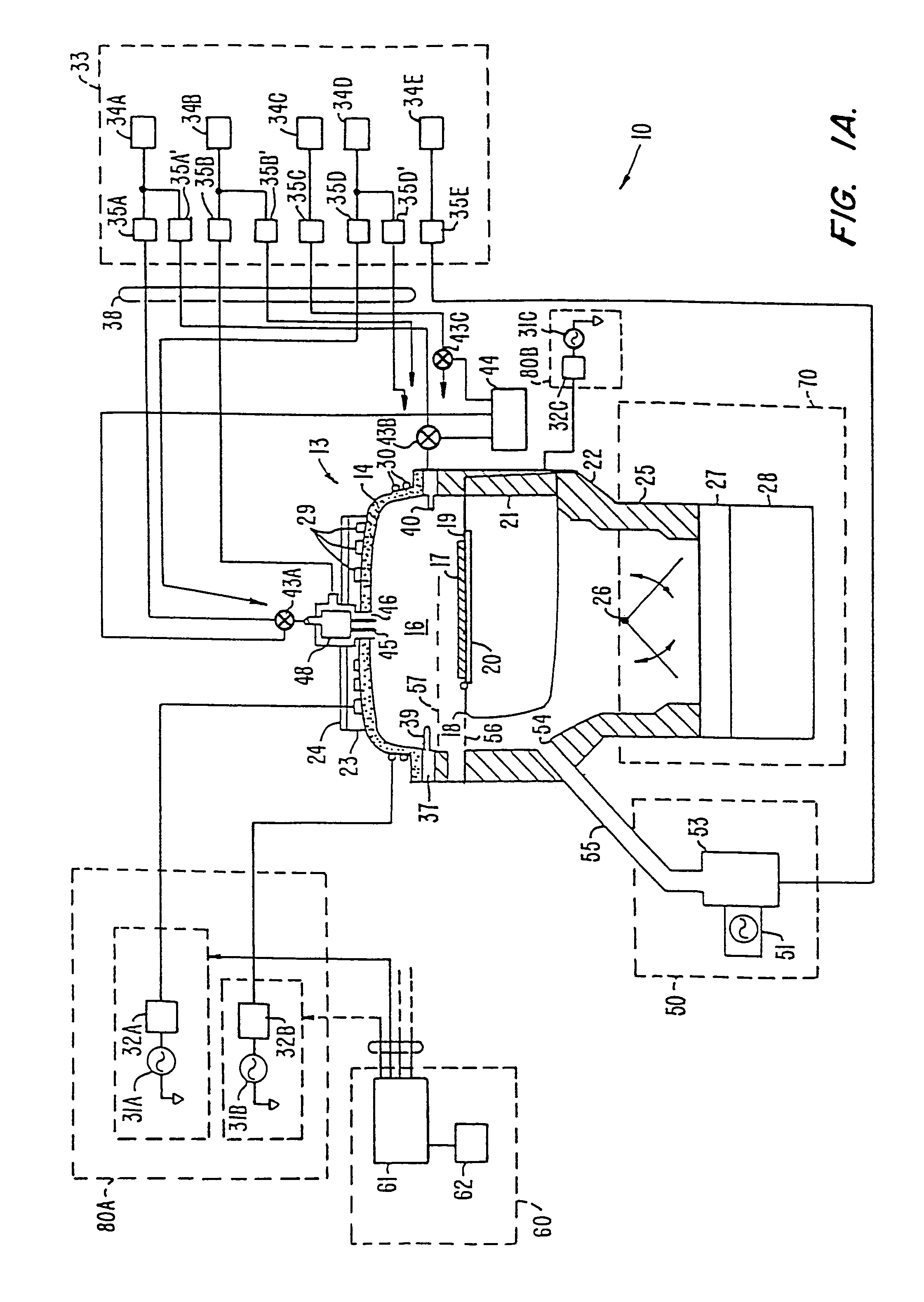
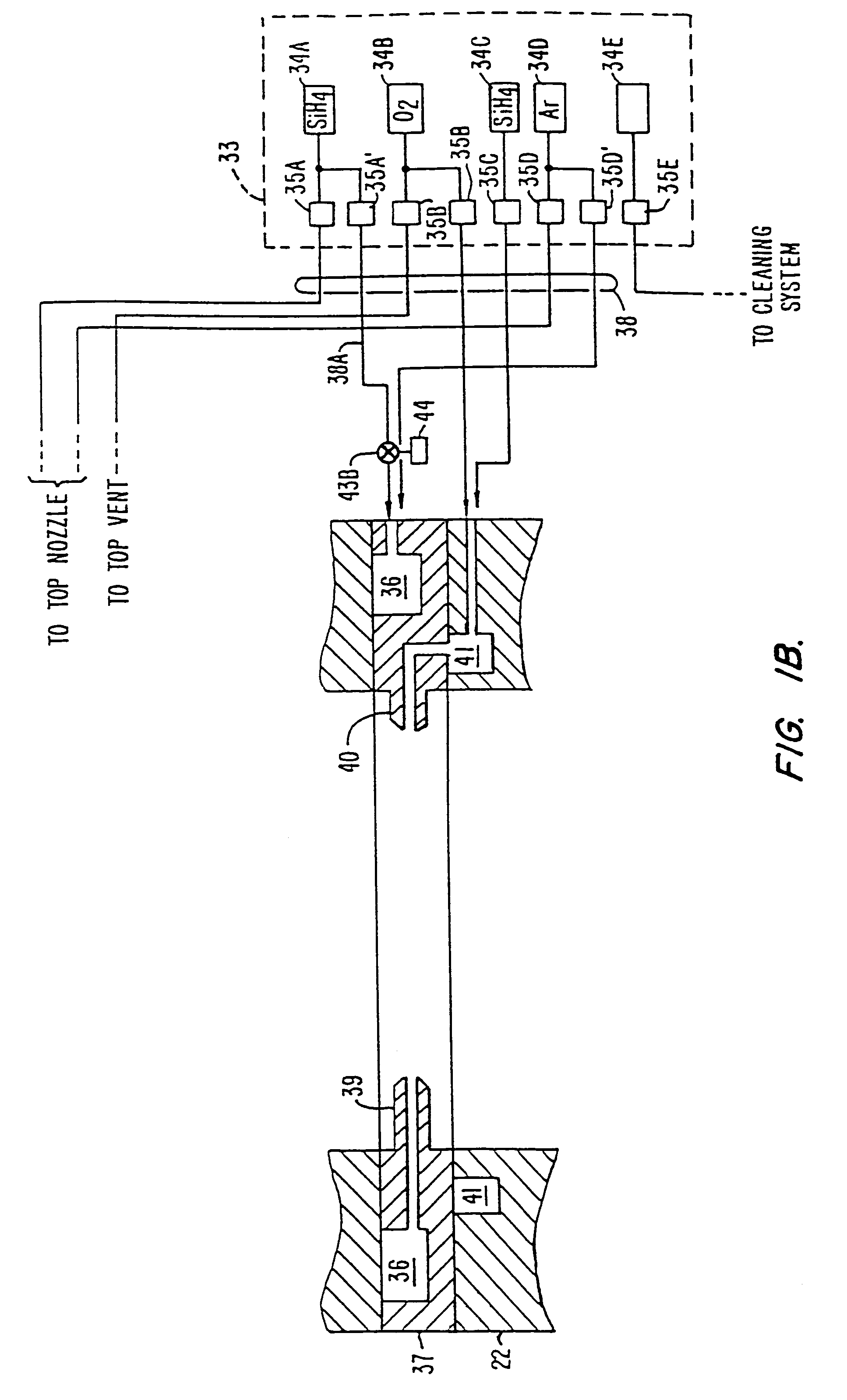
[0023]FIG. 1A illustrates one embodiment of a high density plasma chemical vapor deposition (HDP-CVD) system 10 in which a dielectric layer according to the present invention can be deposited. System 10 includes a chamber 13, a vacuum system 70, a source plasma system 80A, a bias plasma system 80B, a gas delivery system 3...


PUM

PropertyMeasurementUnit
widthaaaaaaaaaa
temperatureaaaaaaaaaa

Abstract

A method and apparatus are disclosed for depositing a dielectric film in a gap having an aspect ratio at least as large as 6:1. By cycling the gas chemistry of a high-density-plasma chemical-vapor-deposition system between deposition and etching conditions, the gap may be substantially 100% filled. Such filling is achieved by adjusting the flow rates of the precursor gases such that the deposition to sputtering ratio during the deposition phases is within certain predetermined limits.

Description

CROSS REFERENCE TO RELATED APPLICATION[0001]This application is a divisional of Ser. No. 09 / 648,395 now U.S. Pat. No. 6,335,288, filed Aug. 24, 2000.BACKGROUND OF THE INVENTION[0002]The present invention relates to the manufacture of integrated circuits on a substrate. More particularly, the invention relates to a method and apparatus for improving the gap-fill capability of high-density-plasma chemical-vapor-deposition techniques.[0003]One of the primary steps in the fabrication of modern semiconductor devices is the formation of a thin film on a semiconductor substrate by chemical reaction of gases. Such a deposition process is referred to as chemical vapor deposition (“CVD”). Conventional thermal CVD processes supply reactive gases to the substrate surface where heat-induced chemical reactions take place to produce a desired film. Plasma-enhanced CVD (“PECVD”) techniques, on the other hand, promote excitation and / or dissociation of the reactant gases by the application of radio-f...

Claims


Application Information

Patent Timeline
Patent Type & Authority Patents(United States)
IPC IPC(8): H01L21/00C23C16/00H01L21/205C23C16/04C23C16/44C23C16/455C23C16/517C23C16/52H01L21/3065H01L21/316H01L21/76H10B12/00
CPCC23C16/045C23C16/45523C23C16/463C23C16/517C23C16/52H01J37/321H01J37/3244H01L21/02164H01L21/02274H01L21/30655H01L21/31608H01L21/31629C23C16/4405Y10S438/911H01J2237/3327H01J2237/3347H01L21/02131
Inventor KWAN, MICHAELLIU, ERIC
Owner APPLIED MATERIALS INC
Learn More