
Method of fabricating non-volatile memory cell adapted for integration of devices and for multiple read/write operations

a non-volatile, memory cell technology, applied in the direction of basic electric elements, electrical apparatus, semiconductor devices, etc., can solve the problems of more serious failures, programming failures, affecting the reliability of devices, etc., and achieve the effect of avoiding the misalignment of the charge trapping layer in the memory cell and improving the operation of the devi

Active Publication Date: 2006-05-23
POWERCHIP SEMICON MFG CORP
View PDF3 Cites 21 Cited by
  • Summary
  • Abstract
  • Description
  • Claims
  • Application Information

AI Technical Summary

Benefits of technology

[0011]The other object of the present invention is to provide a method of fabricating a non-volatile memory cell, which can prevent device failures resulting from the misalignment of the charge trapping layer in the memory cell.
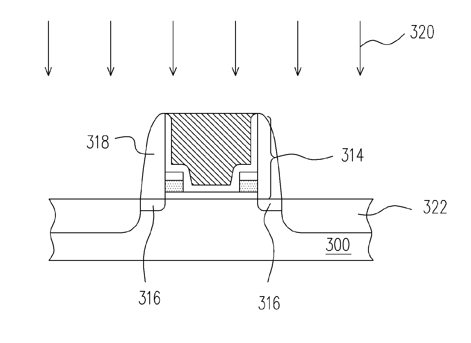
[0014]The present invention separates the charge trapping layer into two independent structures. Accordingly, the present invention is adapted for the integration of devices and for long-time operation.
[0015]Additionally, the present invention uses spacers as a mask for separating the charge trapping layer. Therefore, the misalignment of the charge trapping layer in the memory cell can be avoided, and the operation of the device can be improved.

Problems solved by technology

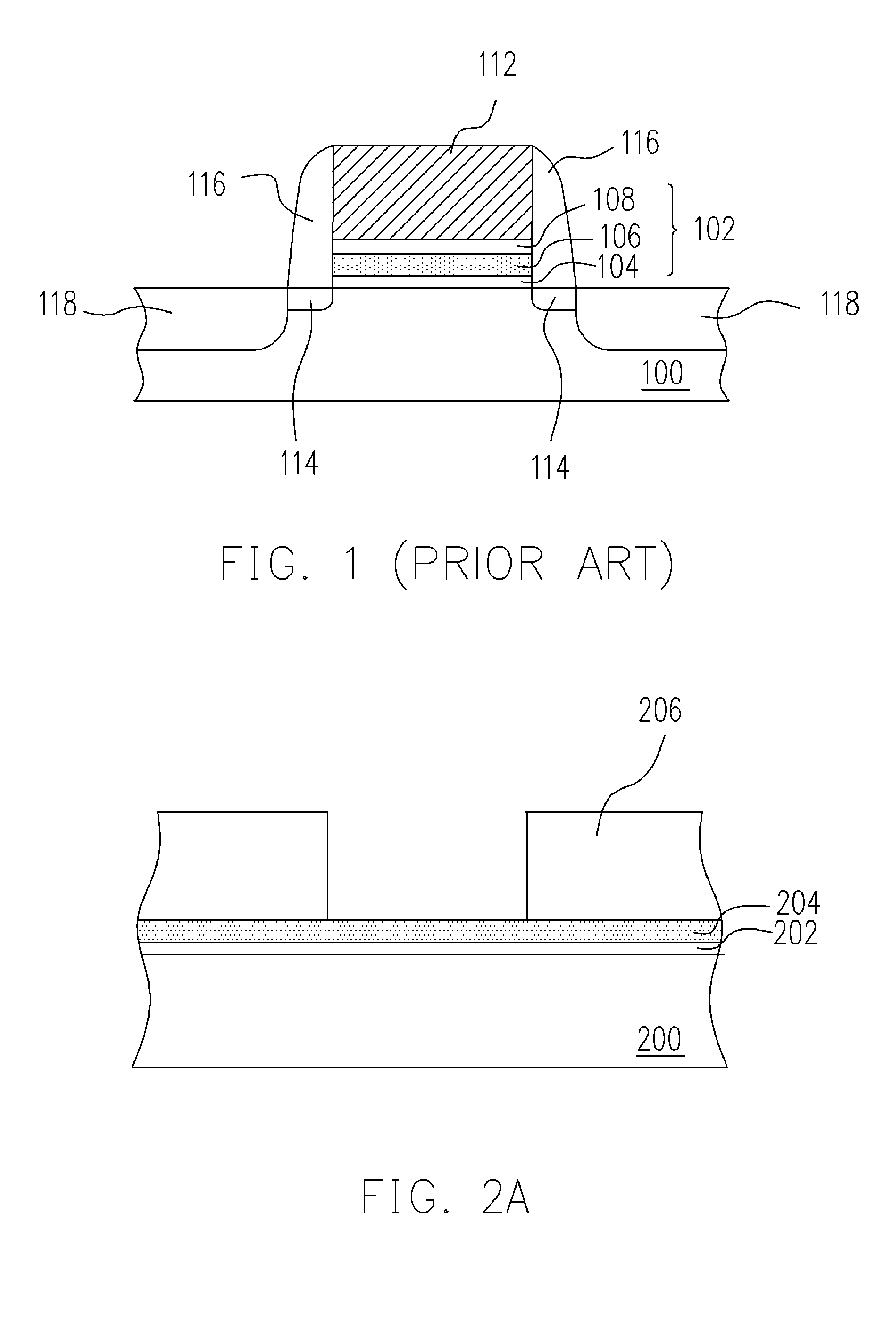
However, when defects exist in the tunneling oxide beneath the polysilicon floating gate, leakage currents occur and affect the reliability of the device.
It results in programming failures.
The failures will be more serious when size of devices shrinks.
However, the silicon nitride spacers formed by the prior art method may directly contact the substrate and the polysilicon layer.
That will cause the operational problems of the memory device.

Method used


Image

  • Method of fabricating non-volatile memory cell adapted for integration of devices and for multiple read/write operations
  • Method of fabricating non-volatile memory cell adapted for integration of devices and for multiple read/write operations
  • Method of fabricating non-volatile memory cell adapted for integration of devices and for multiple read/write operations

Examples


Embodiment Construction

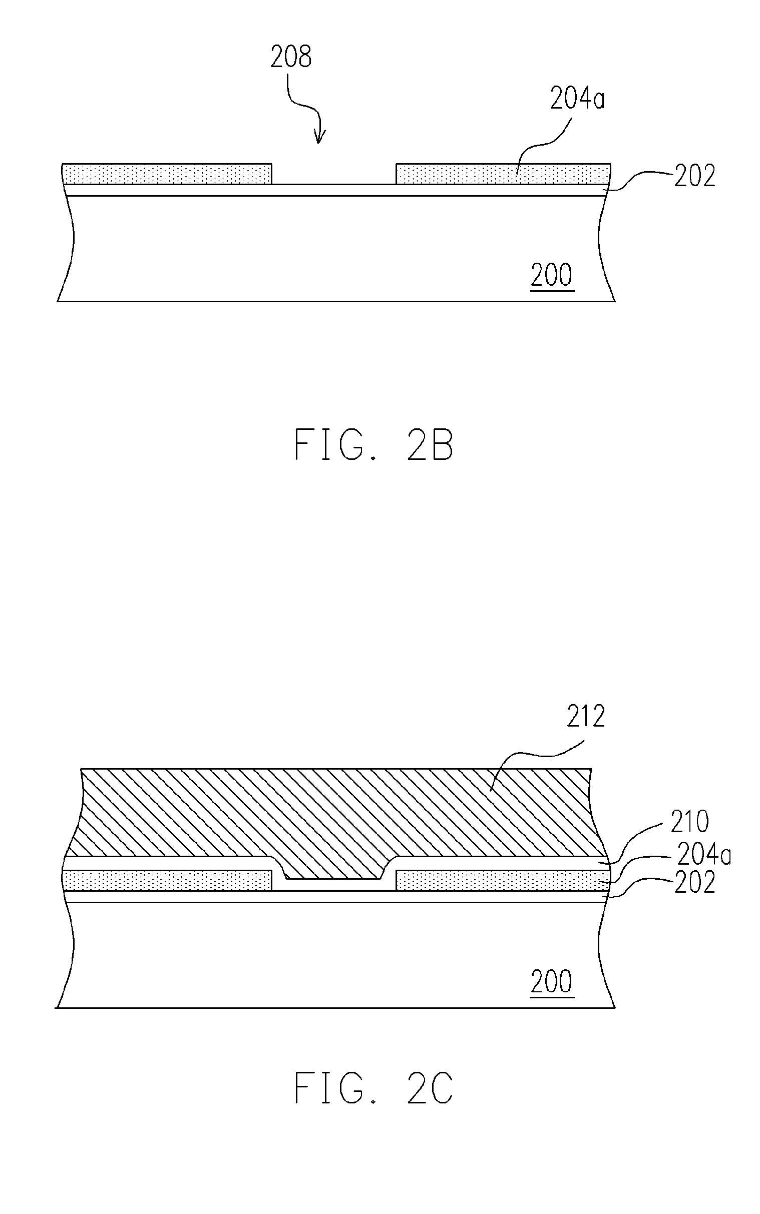
[0020]FIGS. 2A–2E are cross-sectional views showing a first exemplary process flow of fabricating a non-volatile memory cell.

[0021]Please referring to FIG. 2A, a bottom dielectric layer 202 is formed on a substrate 200. The step, for example, forms a silicon oxide layer on the surface of the substrate 200 by a thermal oxidation process. Then, a charge trapping layer 204 is formed on the bottom dielectric layer 204, wherein the material of the charge trapping layer 204 is, for example, selected from a group consisting of silicon nitride, tantalum oxide, SrTiO3 and hafnium oxide. The step of forming the charge trapping layer 204 on the bottom dielectric layer 202 includes, for example, forming a silicon nitride layer on the bottom dielectric layer 202 by a chemical vapor deposition (CVD) process. Then, a patterned photoresist layer 206 is formed on the charge trapping layer 204.

[0022]Please referring to FIG. 2B, the patterned photoresist layer 206 shown in FIG. 2A serves as an etching...


PUM


Abstract

A method of manufacturing a non-volatile memory cell includes forming a bottom dielectric layer and a charge trapping layer on a substrate sequentially. The electron trapping layer is patterned to form a trench exposing a portion of the bottom dielectric layer. A top dielectric layer is formed over the substrate and covers the electron trapping layer and the exposed bottom dielectric layer. A conductive layer is then formed on the top dielectric layer. The conductive layer, the top dielectric layer, the electron trapping layer and the bottom dielectric layer are patterned to form a stacked structure, wherein a width of the stacked structure is larger than a width of the trench. A source / drain region is formed in the substrate adjacent to the edges of the stacked structure. Because the electron trapping layer of the memory cell is divided into two isolation structures according to the invention, it is adapted for the integration of devices and for long-time operation.

Description

BACKGROUND OF INVENTION[0001]1. Field of the Invention[0002]The present invention relates to a method of fabricating a memory cell, and more particularly to a method of fabricating a non-volatile memory cell.[0003]2. Description of the Related Art[0004]In a variety of non-volatile memories, electrically erasable programmable read-only memory (EEPROM) can perform multiple storing, read / write and erasing functions and the data stored therein will not be erased even if the power is shut down. Therefore, it has been a memory device widely used in personal computers and electronic apparatuses. The typical EEPROM uses polysilicon as a floating gate and a control gate. When the memory is programmed, electrons injected into the floating gate will uniformly spread out therein. However, when defects exist in the tunneling oxide beneath the polysilicon floating gate, leakage currents occur and affect the reliability of the device.[0005]In order to resolve the leakage-current issue of EEPROM, a...

Claims


Application Information

Patent Timeline
Patent Type & Authority Patents(United States)
IPC IPC(8): H01L21/8238H01L21/28H01L21/336H01L21/76H01L21/8247H01L29/792
CPCH01L21/28282H01L29/7923H01L29/66833H01L29/40117
Inventor CHANG, KO-HSINGCHANG, SU-YUAN
Owner POWERCHIP SEMICON MFG CORP
Learn More