Semiconductor integrated circuit card manufacturing method, and semiconductor integrated circuit card

a semiconductor integrated circuit and manufacturing method technology, applied in the direction of semiconductor devices, semiconductor/solid-state device details, instruments, etc., can solve the problems of large and low strength of ic cards charged in such ic cards. achieve the effect of less dispersion of seal shape and seal thickness

Inactive Publication Date: 2006-05-09
SONY CORP
View PDF19 Cites 0 Cited by
  • Summary
  • Abstract
  • Description
  • Claims
  • Application Information

AI Technical Summary

Benefits of technology

[0007]In view of such a point, an object of the present invention is to propose a semiconductor integrated circuit chip seal method and a semiconductor integrated circuit chip device capable of providing a semiconductor integrated circuit chip device having extremely high strength and less dispersion of seal shape and seal thickness.
[0008]Furthermore, the present invention is about to propose such a semiconductor integrated circuit card that there is no fear that a semiconductor integrated circuit chip device is damaged or connection of the electrode thereof to the circuit pattern of a substrate comes off, and control of quality and yield thereof is easy.

Problems solved by technology

The IC chip charged in such an IC card has a drawback that the strength thereof is low and dispersion of seal shape and seal thickness thereof is large because it is sealed by the screen printing of resin.
If the strength of the IC chip is low, there is a fear that the IC chip is damaged or the connection of the electrodes of the IC chip to the circuit pattern of a substrate comes off when the IC card is bent by an external pressure.
If the dispersion of the seal shape and the seal thickness of the IC chip is large, it becomes difficult to control the quality and yield of the IC card.

Method used


Image

  • Semiconductor integrated circuit card manufacturing method, and semiconductor integrated circuit card
  • Semiconductor integrated circuit card manufacturing method, and semiconductor integrated circuit card
  • Semiconductor integrated circuit card manufacturing method, and semiconductor integrated circuit card

Examples


Embodiment Construction

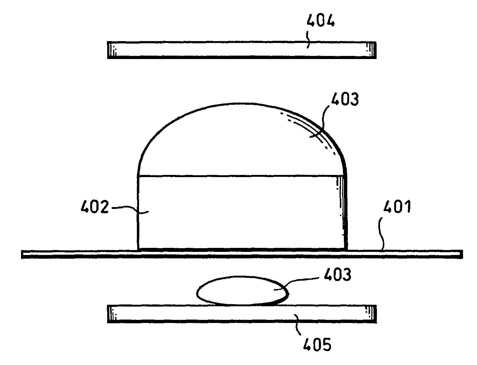
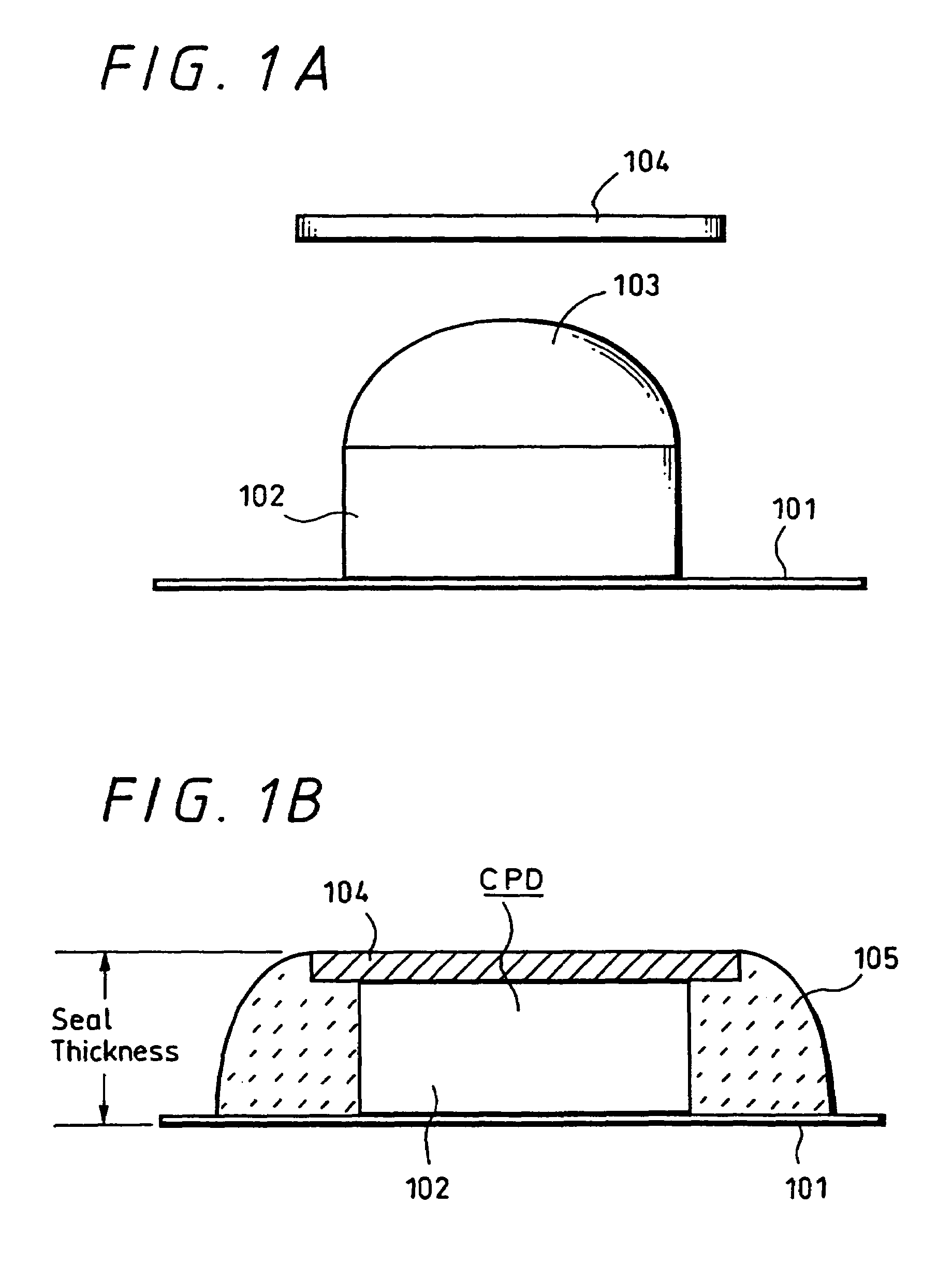
[0017]Hereafter, a semiconductor integrated circuit chip (IC chip) seal method, a semiconductor integrated circuit chip device (IC chip device), and a semiconductor integrated circuit card (IC card), which are concrete examples of the invention, will be described with reference to the drawings.

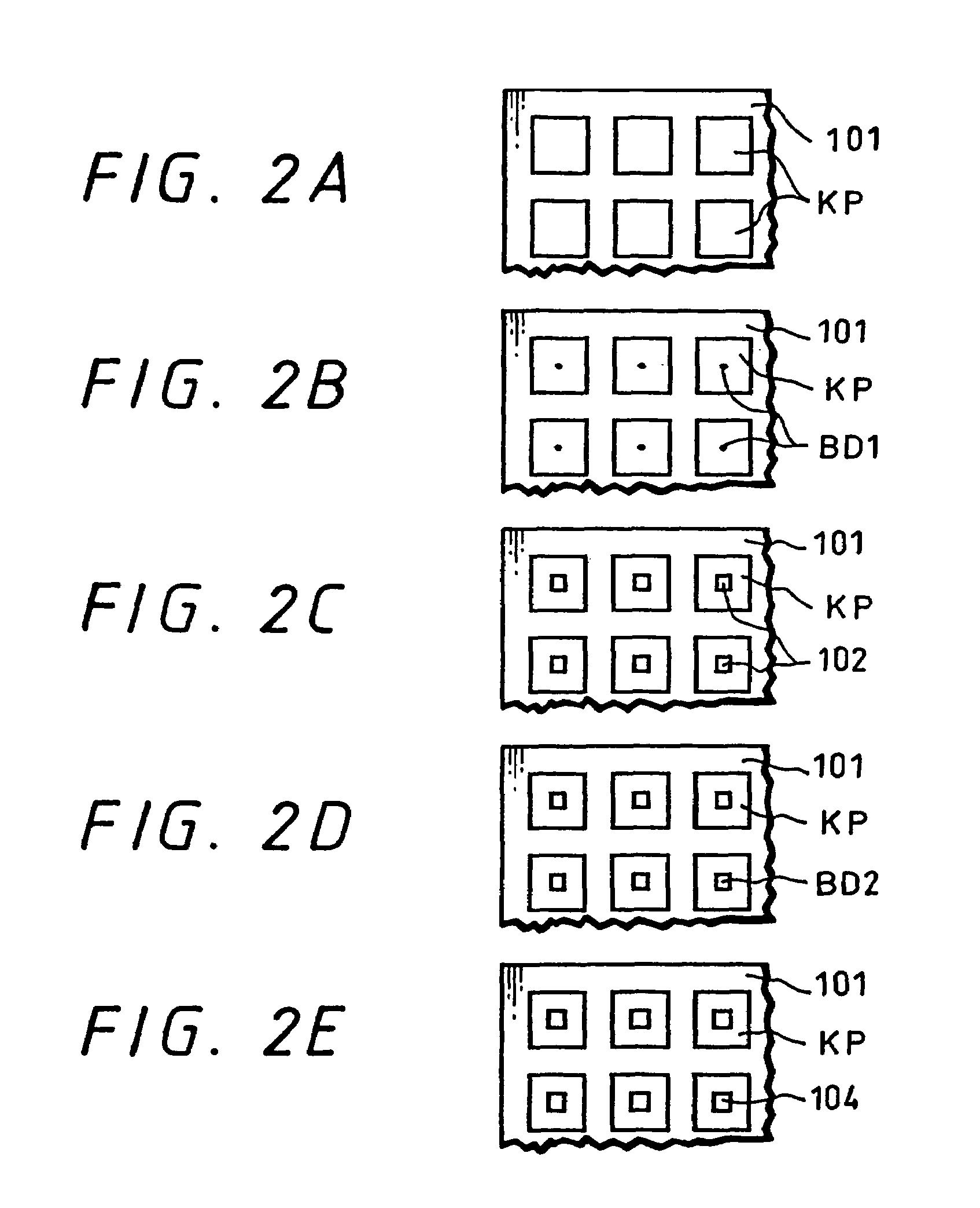
[0018]First of all, with reference to FIGS. 1A, 1B and FIGS. 2A to 2E, an IC chip seal method and an IC chip device (FIG. 1B), which are concrete examples of the present invention, will be described. As shown in FIG. 2A, a film substrate 101 having a plurality of circuit patterns KP formed thereon is prepared. As shown in FIG. 2B, a small quantity of bonding agent BD1 is applied onto each circuit pattern KP of the film substrate 101 or onto the film substrate 101 in each circuit pattern KP of FIG. 2A. As shown in FIG. 2C, an IC chip 102 is placed on the bonding agent BD1 of each circuit pattern KP of the film substrate 101, and each IC chip 102 is pressurized. In addition, each IC chip 102 and...


PUM


Abstract

A semiconductor integrated circuit card is disclosed in which such a semiconductor integrated circuit chip device comprising a substrate having a circuit pattern formed thereon, a semiconductor circuit chip bonded onto the substrate and having an electrode connected to the circuit pattern, a reinforcement metal plate, and a seal resin portion for covering a peripheral face of the semiconductor integrated circuit chip and sticking the reinforcement metal plate onto the semiconductor integrated circuit chip is mounted within a card substrate.

Description

CROSS REFERENCE TO RELATED APPLICATIONS[0001]This patent application is a divisional of U.S. application Ser. No. 09 / 413,594, filed on Jul. 2, 2001 now U.S. Pat. No. 6,765,286, the disclosure of which is herein incorporated by reference.BACKGROUND OF THE INVENTION[0002]1. Field of the Invention[0003]The present invention relates to a semiconductor integrated circuit card manufacturing method and a semiconductor integrated circuit card.[0004]2. Description of the Related Art[0005]A semiconductor integrated circuit chip (IC chip) charged in a semiconductor integrated card (IC card) is sealed by the screen printing of resin.[0006]The IC chip charged in such an IC card has a drawback that the strength thereof is low and dispersion of seal shape and seal thickness thereof is large because it is sealed by the screen printing of resin. If the strength of the IC chip is low, there is a fear that the IC chip is damaged or the connection of the electrodes of the IC chip to the circuit pattern...

Claims


Application Information

Patent Timeline
Patent Type & Authority Patents(United States)
IPC IPC(8): H01L21/44H01L21/46H01L21/48G06K19/077H01L23/16H01L23/31
CPCG06K19/077G06K19/07728G06K19/07745H01L23/16H01L23/3121H01L2924/0002H01L2924/00
Inventor MORIMURA, JINICHIMATSUDA, HIROYA
Owner SONY CORP
Why Eureka
Try Eureka