High speed switching driver

a high-speed switching and driver technology, applied in the direction of lasers, electrical devices, laser details, etc., can solve the problems that the complex circuitry of precision current sources used in precision current sources ordinarily does not lend itself to high-speed adjustments, and achieves efficient transmission of information, fast bias switching, and energy dissipation

Inactive Publication Date: 2006-04-18
GOOGLE TECH HLDG LLC
View PDF28 Cites 13 Cited by
  • Summary
  • Abstract
  • Description
  • Claims
  • Application Information

AI Technical Summary

Benefits of technology

[0004]In an illustrative embodiment, a current is switched through a diode or shunted through an alternate path to selectively bias a diode for transmitting. When the current is switched through the diode, the diode can be biased for generating a light output. A second current can be selectively switched through the diode to modulate a light energy output transmitted from the diode. Based on this configuration, fast bias-switching for generating a modulated laser diode output can be achieved by selectively switching the bias current through the diode or alternate path. Consequently, a solid state device can be controlled to transmit data information after a relatively minimal setup time delay to bias the diode.
[0005]A light output of the diode can be coupled to a fiber to transmit information over an optical network such as a passive optical network or cable television (CATV). In such applications, hi-speed biasing of the diode or multiple diodes can be used to more efficiently transmit information via time division multiplexing. That is, one of multiple diodes can be selectively activated in minimal time to transmit a modulated signal over a fiber network shared by multiple transmitters. The other diodes not transmitting can be almost completely shut down so that they do not interfere with the activated diode.
[0006]A resistor can be disposed in series with the diode to dissipate energy and reduce chirping of the circuit during the “switch over” process of biasing the diode. In one application, the resistor is greater than 20 ohms so that the power output of the diode makes a smooth transition when it is switched or modulated. This resistor can be split into two separate resistors, one in each of the modulation and bias current paths.

Problems solved by technology

Complex circuitry often used in precision current sources ordinarily do not lend themselves to high speed adjustments that would be necessary to rapidly shut off, bias or modulate a diode for transmitting.

Method used


Image

  • High speed switching driver
  • High speed switching driver
  • High speed switching driver

Examples


Embodiment Construction

[0022]A description of preferred embodiments of the invention follows.

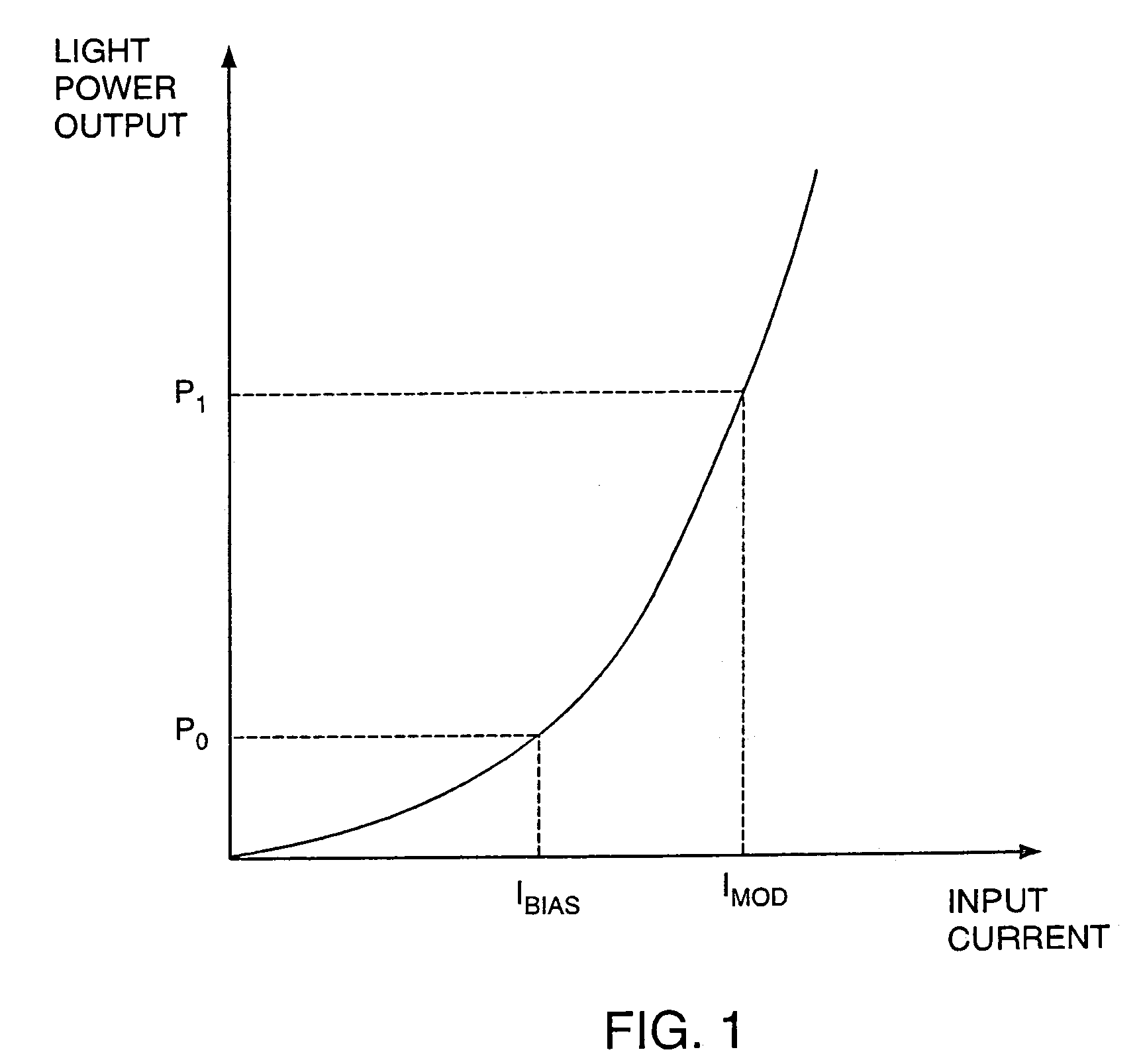
[0023]FIG. 1 is a graph showing the relationship between optical Power and Current (P-I) for a laser diode. As shown, the power output (P) from the laser diode depends on the input pump current (I). As the input pump current (I) reaches a lasing threshold current Ith, the power output P increases rapidly with each successive increase in input pump current I.

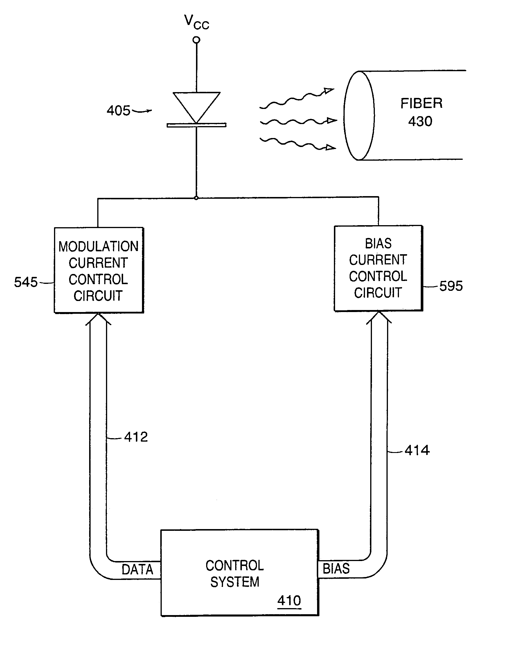
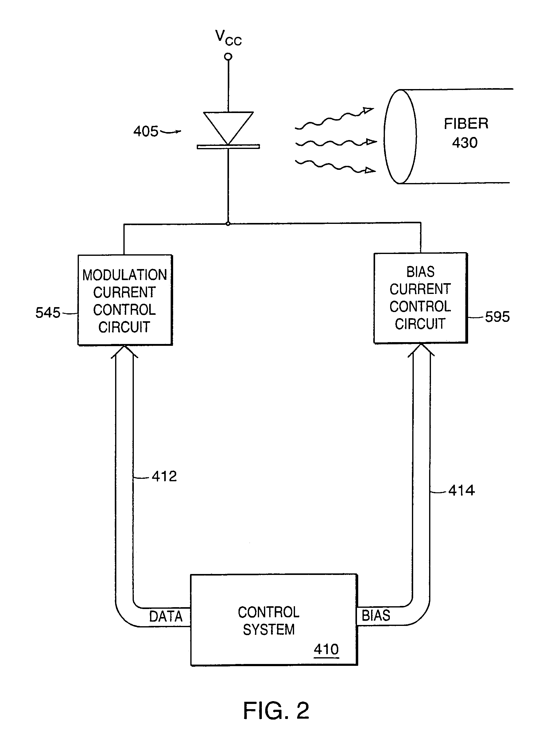
[0024]FIG. 2 is a block diagram of a burst mode laser driver according to certain principles of the present invention. As shown, control system 410 generates data signal 412 and bias signal 414 that respectively drive modulation current control circuit 545 and bias current control circuit 595. A combination of these circuits can be used to control the light output generated by a solid state device such as diode 405. The light output generated by diode 405 can be coupled to fiber 430 of a shared medium network to transmit binary data information.

[0025]Control sy...


PUM


Abstract

The present invention is generally directed towards a system and method for providing a high speed switching driver to transmit data information. A first current is switched through a diode or shunted through an alternate path to selectively bias the diode. A second current can also be selectively switched through the diode to modulate a light energy output transmitted from the diode. Based on this configuration, fast bias-switching for generating a modulated laser diode output can be achieved by selectively switching the bias current through the diode or alternate path. Consequently, a solid state device can be controlled to transmit data information after a relatively minimal setup time delay to bias the diode.

Description

RELATED APPLICATION[0001]This application is a continuation of U.S. application Ser. No. 09 / 975,082, filed Oct. 11, 2001 now U.S. Pat. No. 6,738,401. The entire teachings of the above application are incorporated herein by reference.BACKGROUND OF THE INVENTION[0002]Laser diodes are typically used to transmit data information over fiber optic networks. To achieve higher speed data rates, a laser diode can be biased with a drive current so it is ‘ON’ and produces at least a minimal optical output. While the diode is biased, the diode can be driven with additional current so that the light output of the diode varies over time between two power output levels. One power output level of the diode can represent a logic low while another power output level of the diode can represent a logic high.SUMMARY OF THE INVENTION[0003]One aspect of the present invention is directed towards a system and method for providing high speed switching to transmit data information. This can be achieved by swi...

Claims


Application Information

Patent Timeline
Patent Type & Authority Patents(United States)
IPC IPC(8): H01S3/00H01S5/042H04B10/155
CPCH01S5/042H04B10/504H01S5/0427
Inventor BOWLER, DAVID B.COLELLA, BARRY D.DILL, III, COLBYPRATT, BRUCE C.
Owner GOOGLE TECH HLDG LLC
Why Eureka
Try Eureka