
Microlithographic illumination method and a projection lens for carrying out the method

a technology of projection lens and microlithography, which is applied in the direction of instruments, polarising elements, photomechanical apparatuses, etc., can solve the problems of difficult configuration of systems composed entirely of refractive components that have been sufficiently well-corrected for chromatic aberration, and material photoelastic effects

Inactive Publication Date: 2006-04-18
CARL ZEISS SMT GMBH
View PDF9 Cites 5 Cited by
  • Summary
  • Abstract
  • Description
  • Claims
  • Application Information

AI Technical Summary

Benefits of technology

The solution effectively compensates for imaging errors and maintains consistent image contrast across orientations, improving the quality of patterned devices by ensuring that light rays with orthogonal polarizations traverse equal optical paths, thus reducing variations in image dimensions and contrast.

Problems solved by technology

However, the materials suffer from photoelastic effects, i.e., may affect the mutually orthogonally polarized components of the field vectors of transmitted light differently due to stress birefringence.
Since the Abbé numbers of those materials that are available all lie rather close to one another, it is difficult to configure systems consisting entirely of refractive components that have been sufficiently well-corrected for chromatic aberrations.
However, employing dielectric coatings on optical components that involve large angles of incidence may affect transmitted light in various ways that will depend upon its polarization.

Method used


Image

  • Microlithographic illumination method and a projection lens for carrying out the method
  • Microlithographic illumination method and a projection lens for carrying out the method
  • Microlithographic illumination method and a projection lens for carrying out the method

Examples


Embodiment Construction

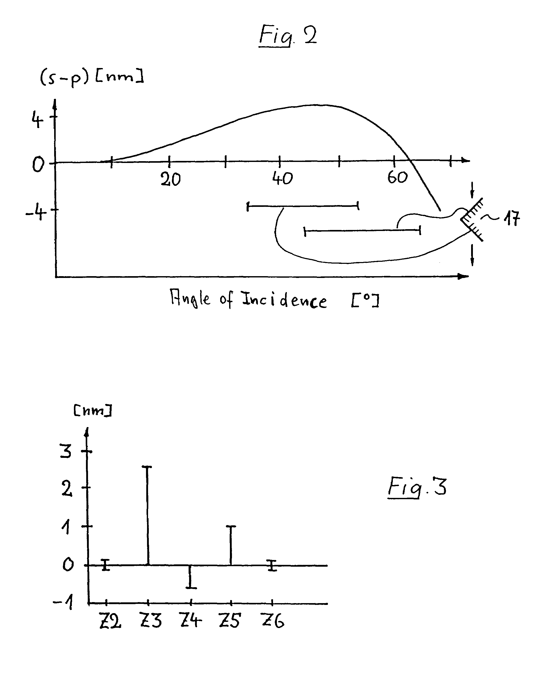
[0047]FIG. 1 schematically depicts a microlithographic projection illumination system 1 in the form of a wafer stepper employed for fabricating VLSI semiconductor de-vices. The projection illumination system includes an excimer laser 2 that serves as its light source. An illumination system 4 generates a large, sharply delimited, and highly uniformly illuminated image field that has been adapted to suit the telecentricity requirements of the projection lens 5 that follows it in the optical train. The illumination system 4 is equipped with means for selecting an illumination mode and is, for example, capable of being switched between conventional illumination with a variable degree of spatial coherence, annular illumination, and dipole or quadrupole illumination. The illumination system is followed by a device 6 for clamping and manipulating a reticle 7 that is arranged such that the reticle lies in the object plane 8 of the projection lens and may be translated along a direction of ...


PUM

PropertyMeasurementUnit
angleaaaaaaaaaa
angleaaaaaaaaaa
wavelengthsaaaaaaaaaa

Abstract

A microlithographic illumination method for imaging a pattern arranged in an object plane of a projection lens onto an image plane of the projection lens, under which a special means for optically correcting the optical path lengths of s-polarized and p-polarized light such that light beams of both polarizations will either traverse essentially the same optical path length between the object plane and the image plane or any existing difference in their optical path lengths will be retained, largely independently of their angles of incidence on the image plane, which will allow avoiding contrast variations due to pattern orientation when imaging finely structured patterns, is disclosed. The contrast variations may be caused by uncorrected projection lenses due to their employment of materials that exhibit stress birefringence and / or coated optical components, such as deflecting mirrors, that are used at large angles of incidence.

Description

[0001]This is a Continuation-In-Part Application of application Ser. No. 10 / 146,915, filed May 17, 2002 now U.S. Pat. No. 6,728,043, which claims benefit of German Patent Application No. 101 24 474.6, filed on May 19, 2001. The disclosure of application Ser. No. 10 / 146,915 is incorporated into this Continuation-In-Part Application by reference.BACKGROUND OF THE INVENTION[0002]1. Field of the Invention[0003]The invention relates to a method for imaging a pattern arranged in an object plane of a projection lens onto an image plane of the projection lens, a projection lens for carrying out the method, and a method for fabricating such a projection lens.[0004]2. Description of the Related Art[0005]Illumination methods and projection lenses of the types are employed on projection illumination systems, such as wafer scanners or wafer steppers, that are used for fabricating semiconductor devices or other types of microelectronic devices and serve to project reduced images of patterns prese...

Claims


Application Information

Patent Timeline
Patent Type & Authority Patents(United States)
IPC IPC(8): G02B27/10G03F7/20
CPCG03F7/70058G03F7/70225G03F7/70966G03F7/70566Y10S359/90
Inventor GRUNER, TORALFMAUL, MANFREDVON BUENAU, RUDOLF
Owner CARL ZEISS SMT GMBH
Learn More