Resin-sealed-type semiconductor device, and production process for producing such semiconductor device

Inactive Publication Date: 2006-04-18
NEC ELECTRONICS CORP
View PDF20 Cites 34 Cited by
  • Summary
  • Abstract
  • Description
  • Claims
  • Application Information

AI Technical Summary

Benefits of technology

[0008]Therefore, a main object of the present invention is to provide a resin-sealed type semiconductor device having an electronic component encapsulated in a molded resin package, and a heat spreader incorporated in the molded resin package to facilitate radiation of heat from the electronic component, wherein an entire thickness of the molded resin package can be reduced without thinning a skin layer of the molded resin package.
[0014]In any event, each of the plate sections may be formed with a plurality of protrusions which are in direct contact with a corresponding uncovered area on the rear surface of the electronic component. Also, each of the plate sections may be further formed with a plurality of openings to thereby facilitate prevalence of resin in a molding cavity for the molded resin package.
[0019]In this production method, the heat spreader includes respective plate sections which cover the uncovered areas on the rear surface of the electronic component. Also, each of the plate sections is formed with a plurality of protrusions which are in direct contact with a corresponding uncovered area on the rear surface of the electronic component. Each of the plate sections may be further formed with a plurality of openings to thereby facilitate prevalence of the uncured resin in the complete molding cavity for the molded resin package.

Problems solved by technology

Of course, the incorporation of the heat spreader in the molded resin package results in an increase in an entire thickness of the molded resin package, and this is contrary to the trend in which the thickness of resin-sealed type semiconductor devices should be made as small as possible.
Otherwise, wiring patterns, included in the molded resin package, are subjected to premature corrosion.
In any event, conventionally, there are no proposals for reducing the entire thickness of the molded resin package without thinning the skin layer of the molded resin package.

Method used


Image

  • Resin-sealed-type semiconductor device, and production process for producing such semiconductor device
  • Resin-sealed-type semiconductor device, and production process for producing such semiconductor device
  • Resin-sealed-type semiconductor device, and production process for producing such semiconductor device

Examples


Embodiment Construction

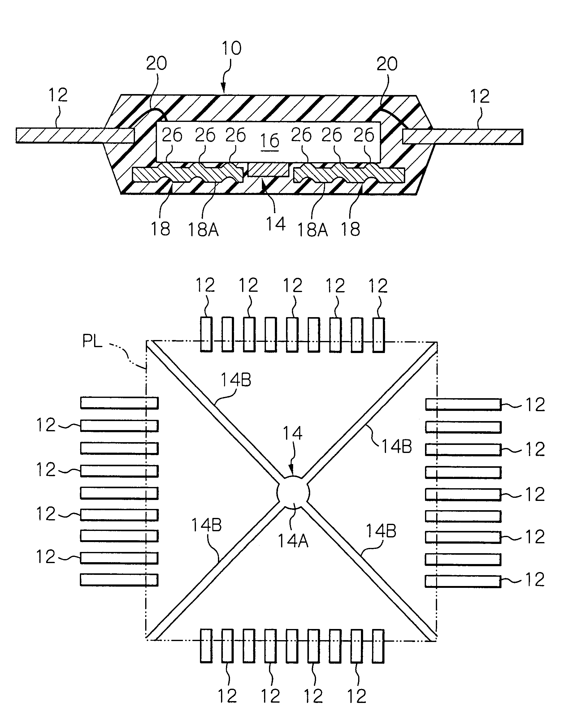
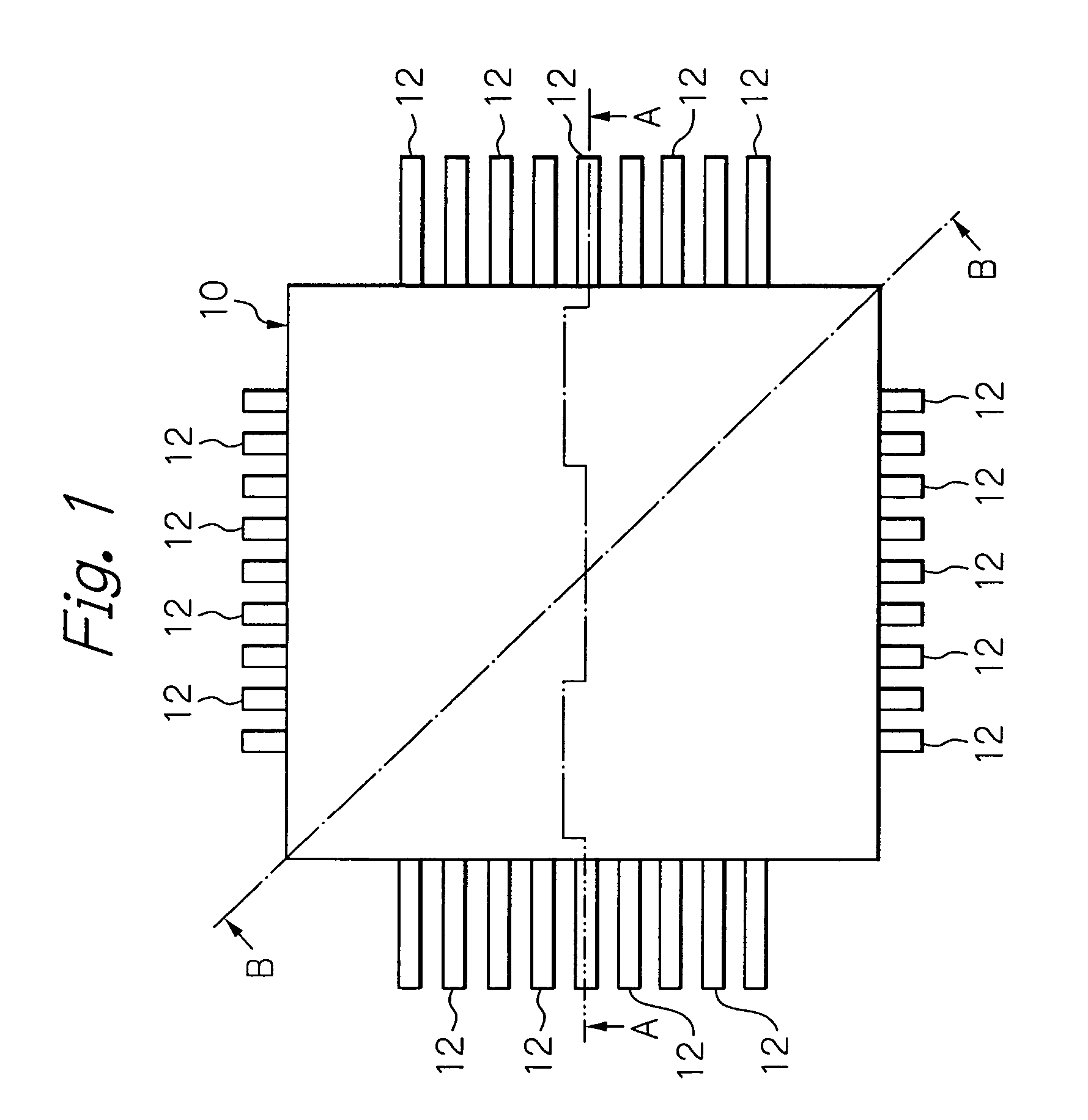
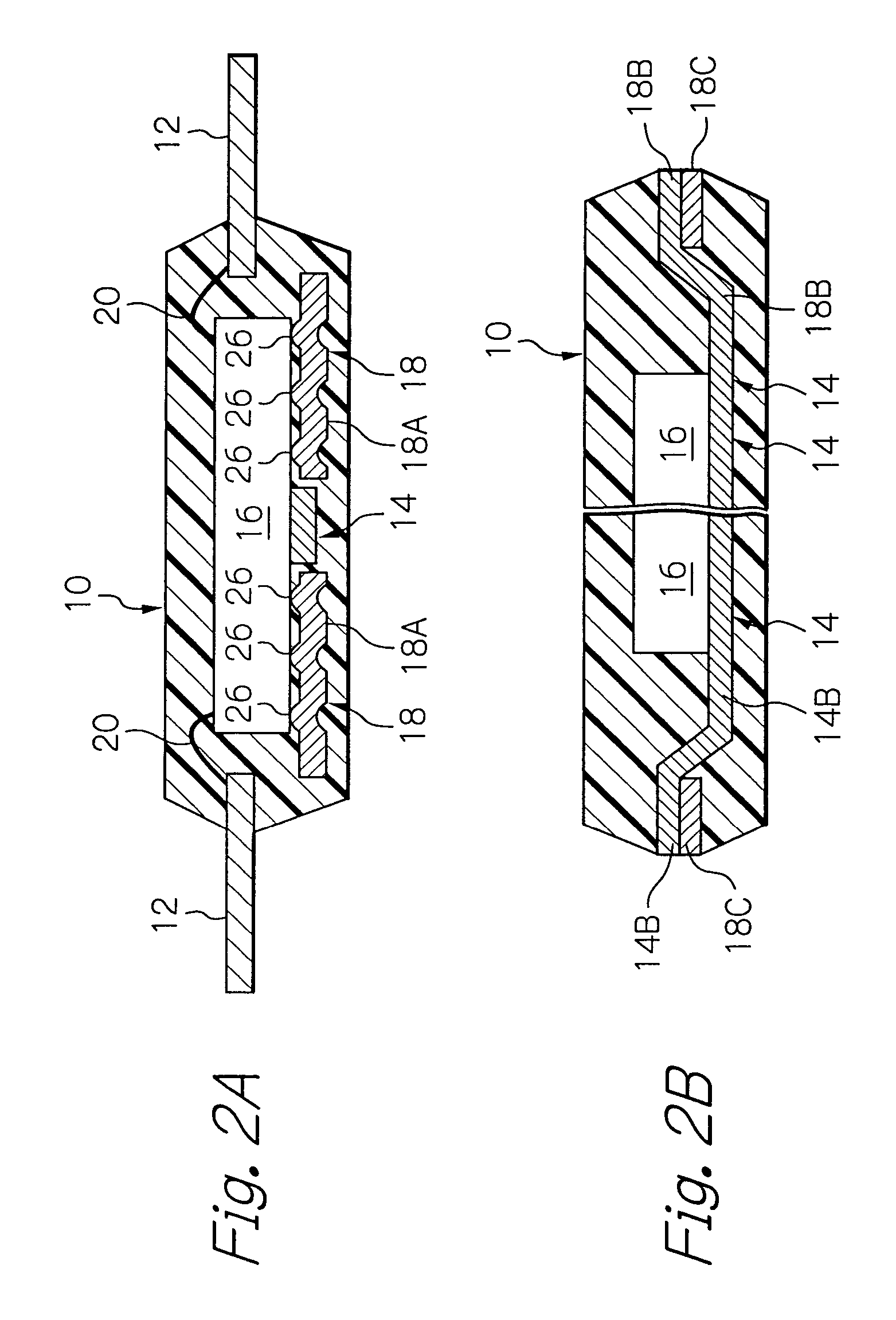
[0040]First, with reference to FIG. 1, an embodiment of a resin-sealed type semiconductor device according to the present invention is illustrated in a plan view, and FIGS. 2A and 2B show respective cross sections of the resin-sealed type semiconductor device, taken along the A—A and B—B lines of FIG. 1.

[0041]As is apparent from FIG. 1, the resin-sealed type semiconductor device includes a molded resin package 10 having a rectangular configuration, and a plurality of leads 12 projecting from the sides of the molded resin package 10, and each of the leads 12 has an inner lead section buried in the molded resin package 10. As shown in FIGS. 2A and 2B, the resin-sealed type semiconductor device further includes a mount stage 14, an electronic component 16 mounted on the mount stage 14 so as to be in contact with a rear surface thereof, and a heat spreader 18 associated with the mount stage 12 and the electronic component 16, and the mount stage 14, the electronic component 16, and the ...


PUM


Abstract

A resin-sealed type semiconductor device has a mount stage, a semiconductor chip mounted on the stage such that a rear surface of the chip is in contact with the stage, a heat spreader associated with the stage and the chip, and a molded resin package encapsulating the stage, chip, and heat spreader. The stage is configured such that the rear surface of the chip is partially covered with the stage, whereby uncovered areas are defined on the rear surface of the electronic component. The heat spreader is complementarily configured with respect to the stage so as to be in direct contact with the uncovered areas of the rear surface of the electronic component, whereby an entire thickness of both the mount stage and the heat spreader is smaller than a total of a thickness of the mount stage and a thickness of the heat spreader.

Description

BACKGROUND OF THE INVENTION[0001]1. Field of the Invention[0002]The present invention relates to a resin-sealed type semiconductor device having an electronic component encapsulated in a molded resin package, and a heat spreader incorporated in the molded resin package to facilitate radiation of heat from the electronic component, and also relates to a production method for manufacturing such a resin-sealed type semiconductor device.[0003]2. Description of the Related Art[0004]In general, a resin-sealed type semiconductor device is produced by using a lead frame including a mount stage and a plurality of leads. In particular, first, an electronic component, such as a semiconductor chip, is mounted on the mount stage, and then the respective leads are electrically connected at their inner ends to terminal pads formed and arranged on the electronic component through bonding wires. Subsequently, the electronic component is placed together with the mount stage in a molding cavity define...

Claims


Application Information

Patent Timeline
IPC IPC(8): H01L23/28H01L23/34H01L21/56H01L23/433H01L23/495H01L23/50
CPCH01L21/565H01L23/49503H01L24/32H01L23/4334H01L24/78H01L2924/01006H01L2224/32057H01L2224/32245H01L2224/48091H01L2224/48247H01L2224/48465H01L2224/73265H01L2224/83385H01L2924/01004H01L2924/01013H01L2924/01029H01L2924/01033H01L2924/01082H01L2224/78H01L2224/45124H01L2924/01072H01L24/48H01L2924/01005H01L2924/00014H01L2924/00H01L2924/00011H01L2924/181H01L2224/45099H01L2924/00012H01L2924/01049H01L23/34
Inventor KIMURA, NAOTO
Owner NEC ELECTRONICS CORP
Why Eureka
Try Eureka