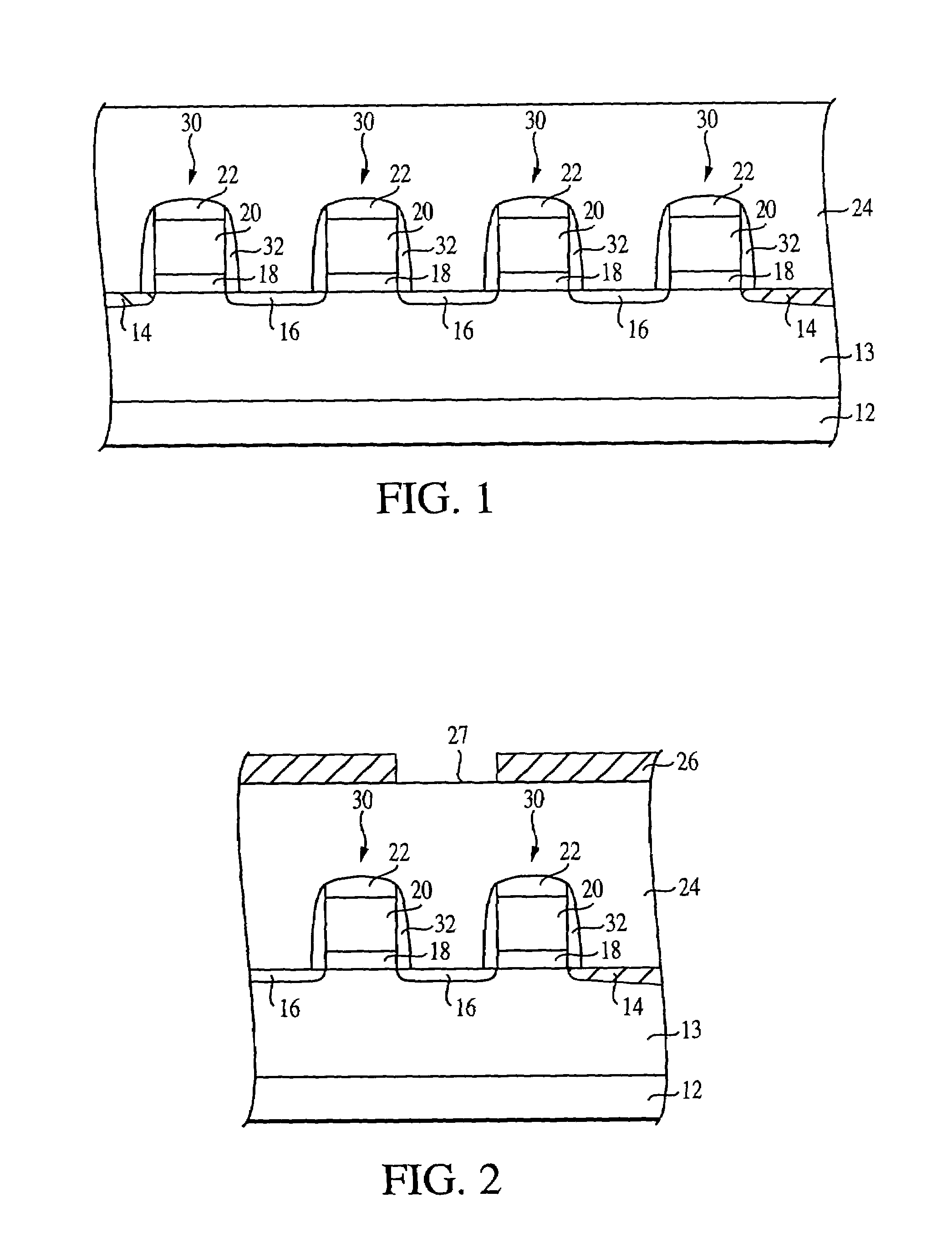
Method of forming MIS capacitor
a capacitor and mis-forming technology, applied in the field of integrated circuits, can solve the problems of increasing the packing density of cell capacitors at the expense of the available cell area, difficulty in providing sufficient capacitance using conventional stacked capacitor structures, and technical difficulties associated with these materials, so as to improve the cell capacitance and leakage, reduce leakage current, and high capacitance
- Summary
- Abstract
- Description
- Claims
- Application Information
AI Technical Summary
Benefits of technology
Problems solved by technology
Method used
Image

Examples
first embodiment
[0087]Under a third set of experiments, a first Al2O3 MIS capacitor was formed on a semiconductor wafer according to the present invention. The first Al2O3 MIS capacitor was fabricated with a lower electrode of CVD hemispherical grained polysilicon of about 400 Angstroms thick, an ALD Al2O3 dielectric layer of about 55 Angstroms thick, and an upper electrode of CVD titanium nitride of about 200 Angstroms thick.
[0088]The ALD Al2O3 dielectric layer of the first Al2O3 MIS capacitor was formed by atomic layer deposition using trimetyl-aluminum (TMA) as an aluminum source precursor and water. The titanium nitride upper electrode was formed by chemical vapor deposition, employing TiCl4 (titanium tetrachloride) as precursor and ammonia (NH3) as nitrogen source.
[0089]A third group of measurements for the capacitance and leakage current of the first Al2O3 MIS capacitor described above was conducted from various die locations across the wafer. The capacitance measurements were conducted at 1 ...
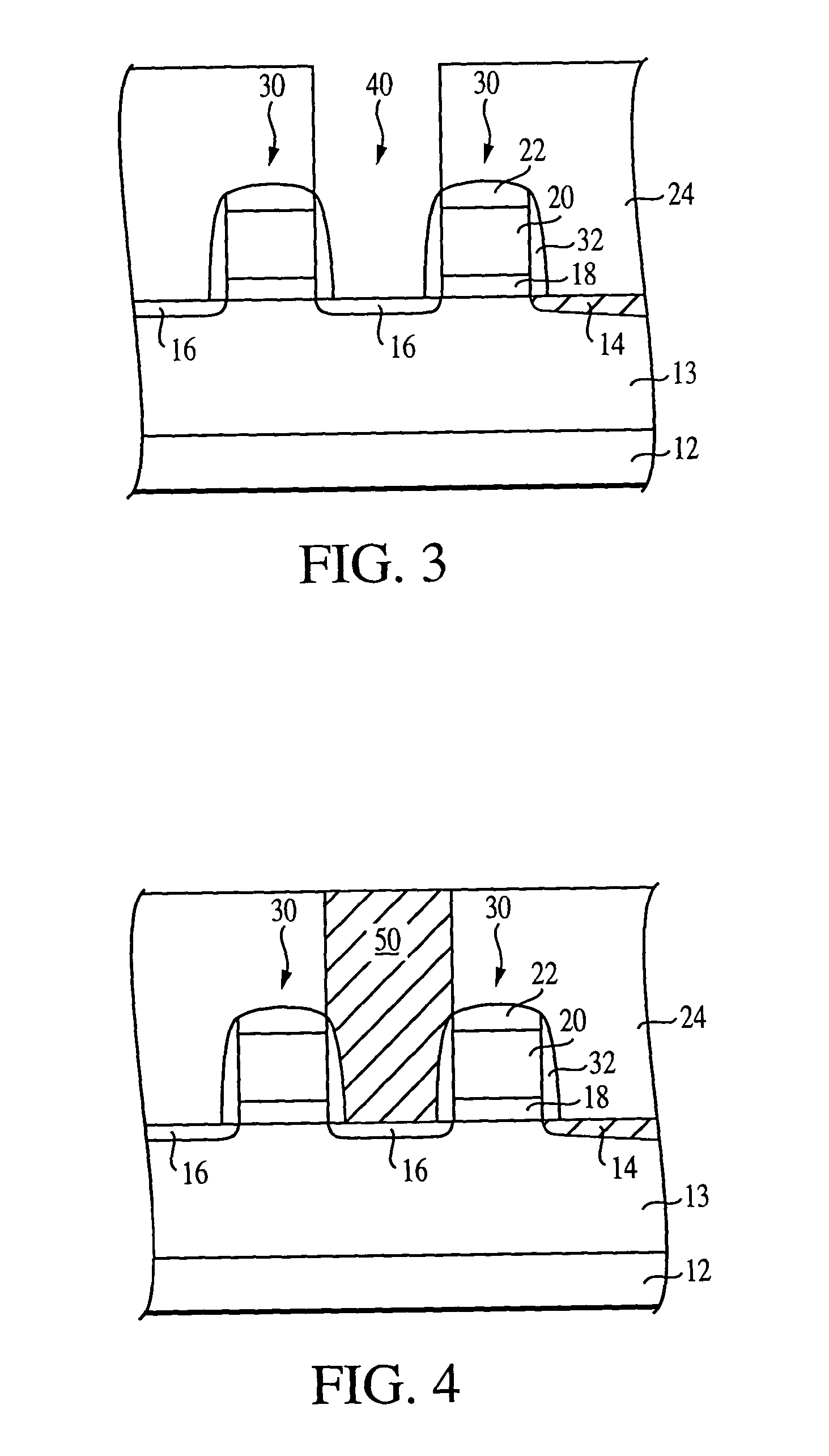
second embodiment
[0091]Under a fourth set of experiments, a second Al2O3 MIS capacitor was formed on a semiconductor wafer according to the present invention. The second Al2O3 MIS capacitor was fabricated with a lower electrode of CVD deposited hemispherical grained polysilicon of about 400 Angstroms thick, an ALD Al2O3 dielectric layer of about 55 Angstroms thick subjected to a post-Al2O3 deposition treatment, and an upper electrode of CVD titanium nitride of about 200 Angstroms thick.
[0092]The ALD Al2O3 dielectric layer of the second Al2O3 MIS capacitor was formed by atomic layer deposition using trimetyl-aluminum (TMA) as an aluminum source precursor and water. The titanium nitride upper electrode was formed by chemical vapor deposition, employing TiCl4 (titanium tetrachloride) as precursor and ammonia (NH3) as a nitrogen source.
[0093]Prior to the formation of the ALD Al2O3 dielectric layer, the lower HSG electrode of the second Al2O3 MIS capacitor was subjected to the following sequence of treat...
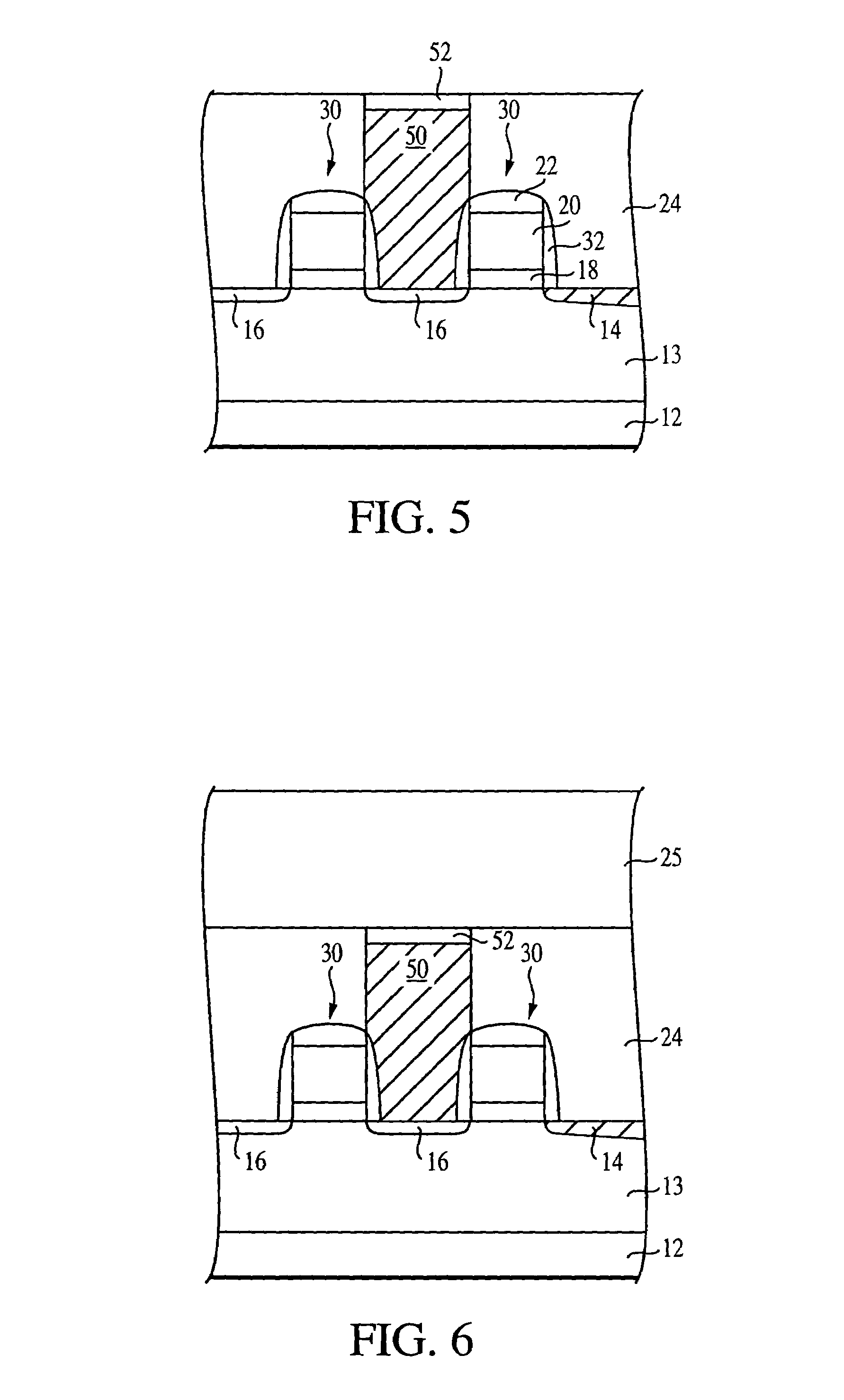
third embodiment
[0096]Under a fifth set of experiments, a third Al2O3 MIS capacitor was formed on a semiconductor wafer according to the present invention. The third Al2O3 MIS capacitor was fabricated with a lower electrode of CVD deposited hemispherical grained polysilicon of about 400 Angstroms thick, an ALD Al2O3 dielectric layer of about 50 Angstroms thick and subjected to a reoxidation treatment, and an upper electrode of CVD titanium nitride of about 200 Angstroms thick.
[0097]The ALD Al2O3 dielectric layer of the third Al2O3 MIS capacitor was formed by atomic layer deposition using trimethyl-aluminum (TMA) as an aluminum source precursor and water. Subsequent to its formation, the ALD Al2O3 dielectric layer of the third Al2O3 MIS capacitor was subjected to a post-deposition oxidation treatment. This way, the ALD Al2O3 dielectric layer underwent an oxidizing ambient under an ozone treatment at about 475° C. for about 3 minutes. The titanium nitride upper electrode was formed by chemical vapor ...
PUM
 Abstract
Description
Claims
Application Information
 - R&D
- Intellectual Property
- Life Sciences
- Materials
- Tech Scout
- Unparalleled Data Quality
- Higher Quality Content
- 60% Fewer Hallucinations
Browse by: Latest US Patents, China's latest patents, Technical Efficacy Thesaurus, Application Domain, Technology Topic, Popular Technical Reports.
© 2025 PatSnap. All rights reserved.Legal|Privacy policy|Modern Slavery Act Transparency Statement|Sitemap|About US| Contact US: help@patsnap.com