Array of light-emitting OLED microcavity pixels
a microcavity and display device technology, applied in the direction of discharge tube/lamp details, thermoelectric devices, discharge tubes, etc., can solve the problems of reducing the efficiency of light-emitting oled, so as to achieve a large color gamut display and low white power consumption
- Summary
- Abstract
- Description
- Claims
- Application Information
AI Technical Summary
Benefits of technology
Problems solved by technology
Method used
Image
Examples
example 3 (
INVENTIVE)
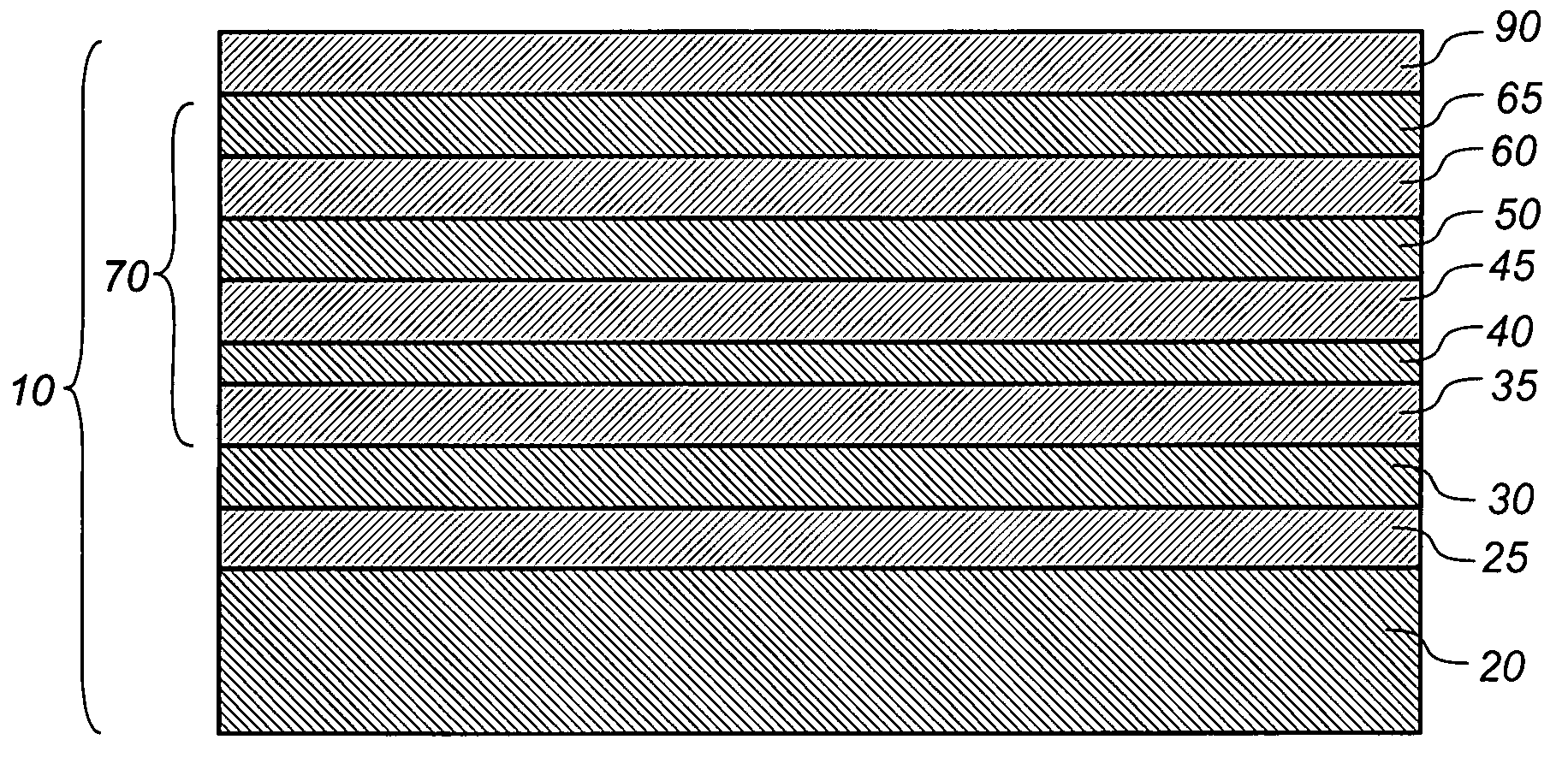
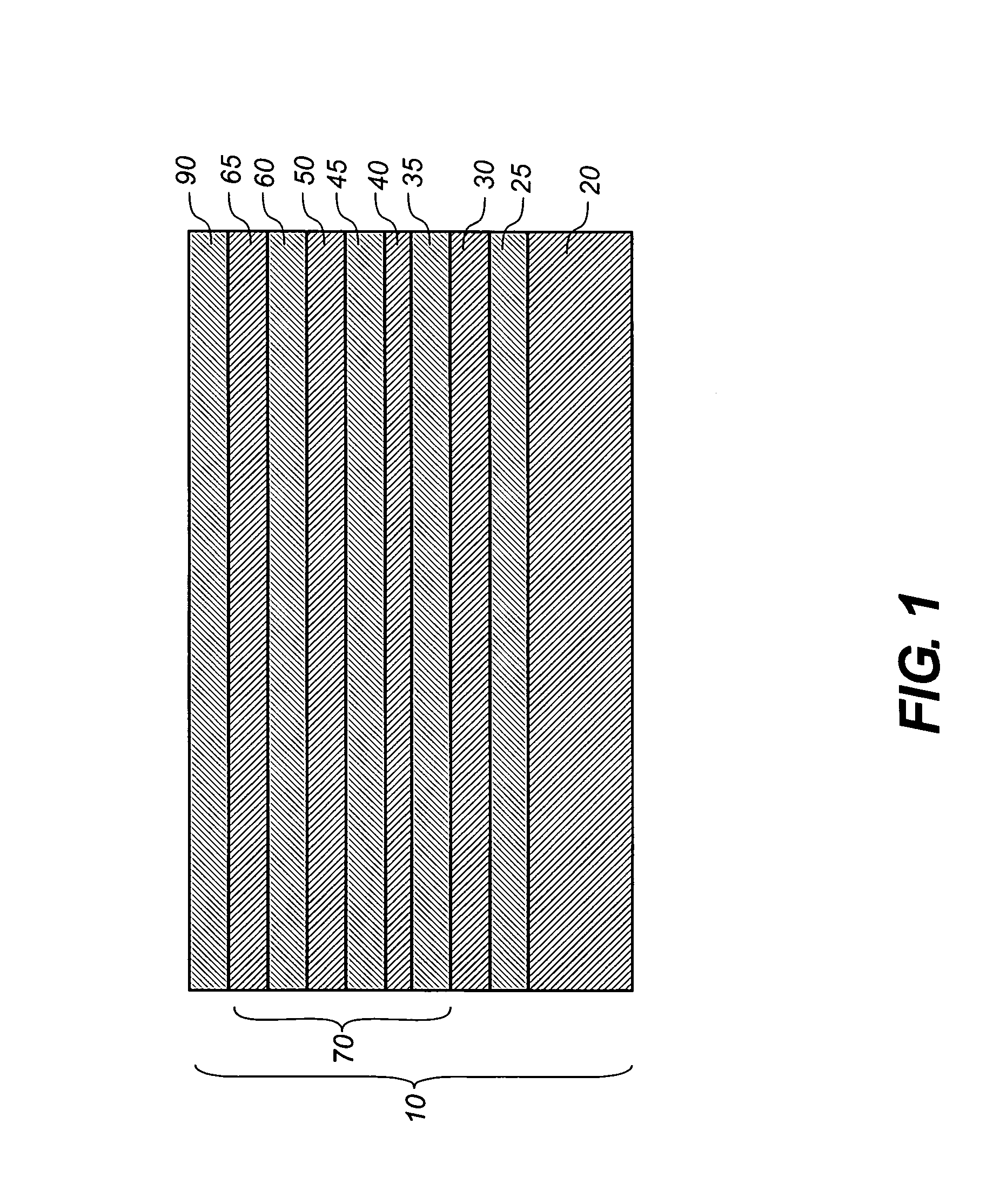
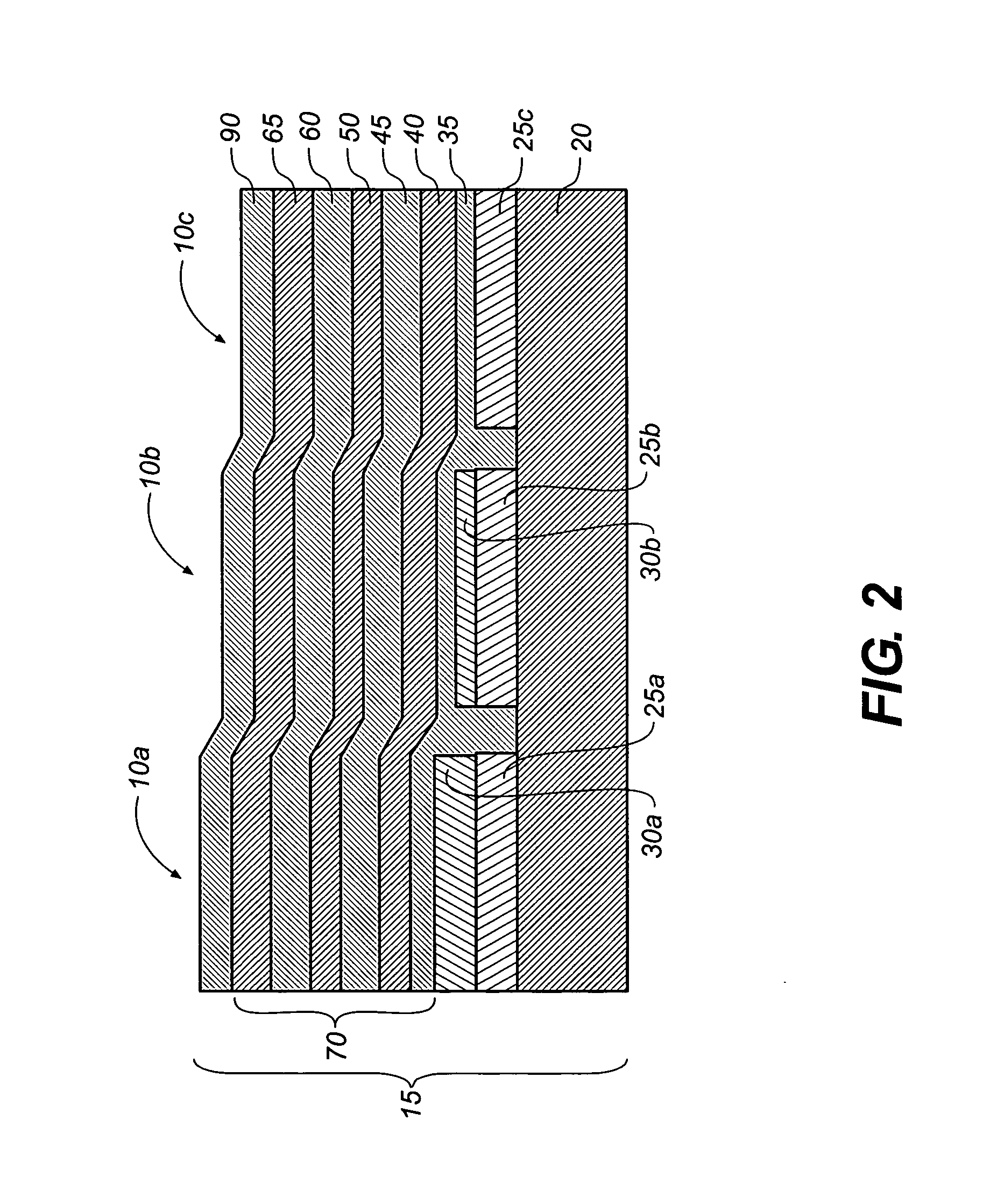
[0234]An inventive color OLED display was constructed in the following manner:[0235]1. A clean glass substrate was deposited by sputtering with indium tin oxide (ITO) to form a transparent electrode of 85 nm thickness;[0236]2. The above-prepared ITO surface was treated with a plasma oxygen etch, followed by plasma deposition of a 0.1 nm layer of a fluorocarbon polymer (CFx) as described in U.S. Pat. No. 6,208,075;[0237]3. The above-prepared substrate was further treated by vacuum-depositing a 90 nm layer of NPB as a hole-transporting layer (HTL);[0238]4. A 150 nm layer having a mixture of 107 nm NPB and 43 nm rubrene containing 0.5% by volume TPDPB (above) was vacuum-deposited onto the substrate at a coating station that included a heated graphite boat source to form a red light-emitting layer (red LEL);[0239]5. A coating having a mixture of 40 nm of TBADN with 4 nm NPB and 3% by volume L47 was evaporatively deposited on the above substrate to form a blue and green light-e...
example 4 (
INVENTIVE)
[0241]An inventive color OLED display was constructed in the manner described in Example 3, except that the following steps were changed:[0242]3. The above-prepared substrate was further treated by vacuum-depositing a 260 m layer of NPB as a hole-transporting layer (HTL);[0243]4. A layer of 30 nm NPB containing 3.5% by volume L50 (above) was vacuum-deposited onto the substrate at a coating station that included a heated graphite boat source to form a red light-emitting layer (red and yellow LEL);[0244]5. A coating having a mixture of 42 nm of BNA (above) with 3 nm NPB and 1% by volume BEP was evaporatively deposited on the above substrate to form a blue light-emitting layer (blue LEL); and[0245]6. A 10 nm electron-transporting layer (ETL) of ALQ was vacuum-deposited onto the substrate at a coating station that included a heated graphite boat source.
[0246]The devices were tested by applying a current across the electrodes of 20 mA / cm2 and measuring the emission spectrum. Th...
PUM
| Property | Measurement | Unit |
|---|---|---|
| wavelength range | aaaaa | aaaaa |
| wavelength range | aaaaa | aaaaa |
| full width at half maximum | aaaaa | aaaaa |
Abstract
Description
Claims
Application Information
 - R&D Engineer
- R&D Manager
- IP Professional
- Industry Leading Data Capabilities
- Powerful AI technology
- Patent DNA Extraction
Browse by: Latest US Patents, China's latest patents, Technical Efficacy Thesaurus, Application Domain, Technology Topic, Popular Technical Reports.
© 2024 PatSnap. All rights reserved.Legal|Privacy policy|Modern Slavery Act Transparency Statement|Sitemap|About US| Contact US: help@patsnap.com


