
Variable programming of non-volatile memory

a non-volatile memory and variable programming technology, applied in static storage, digital storage, instruments, etc., can solve the problems of unselected cells, inadvertent programming, low boosting potential, etc., to improve data retention, reduce program disturbance, and increase step size

Active Publication Date: 2006-03-28
SANDISK TECH LLC
View PDF42 Cites 835 Cited by
  • Summary
  • Abstract
  • Description
  • Claims
  • Application Information

AI Technical Summary

Benefits of technology

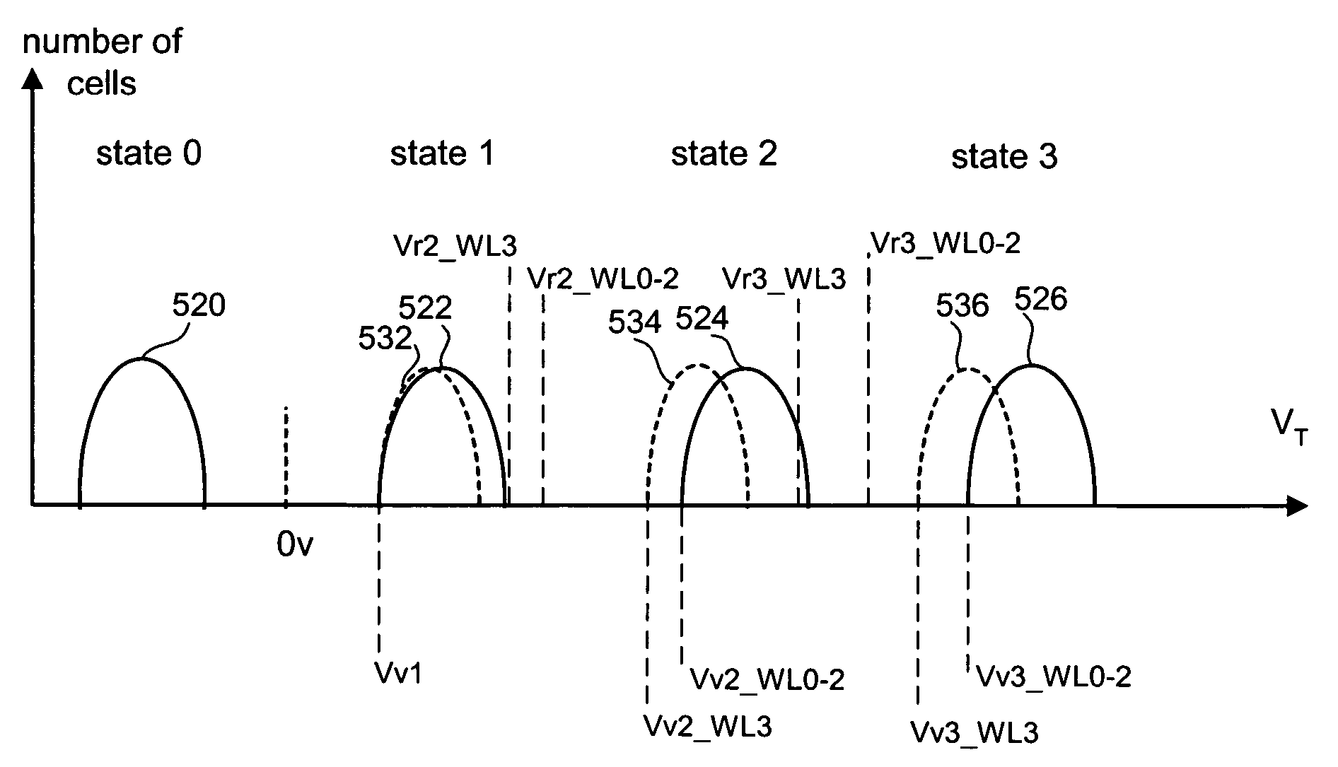
The present invention relates to technology for programming, verifying programming, and reading non-volatile storage elements in a memory device. The invention utilizes variable program target levels, verify levels, read levels, and step sizes when programming, verifying, and reading selected storage elements. By using smaller program voltages to program select storage elements to target physical states, the invention reduces program disturb and improves data retention in the memory device. The invention also includes a method of programming non-volatile memory by programming a first set of storage elements to a first physical state and programming a second set of storage elements to the first physical state using a second target level, where the second target level is below the first target level. The invention also includes a system in accordance with an embodiment of the present invention, which includes an array of storage elements and a managing circuit that performs the steps discussed above. The technical effects of the invention include reduced program disturb, better data retention, and increased programming speed in a memory device.

Problems solved by technology

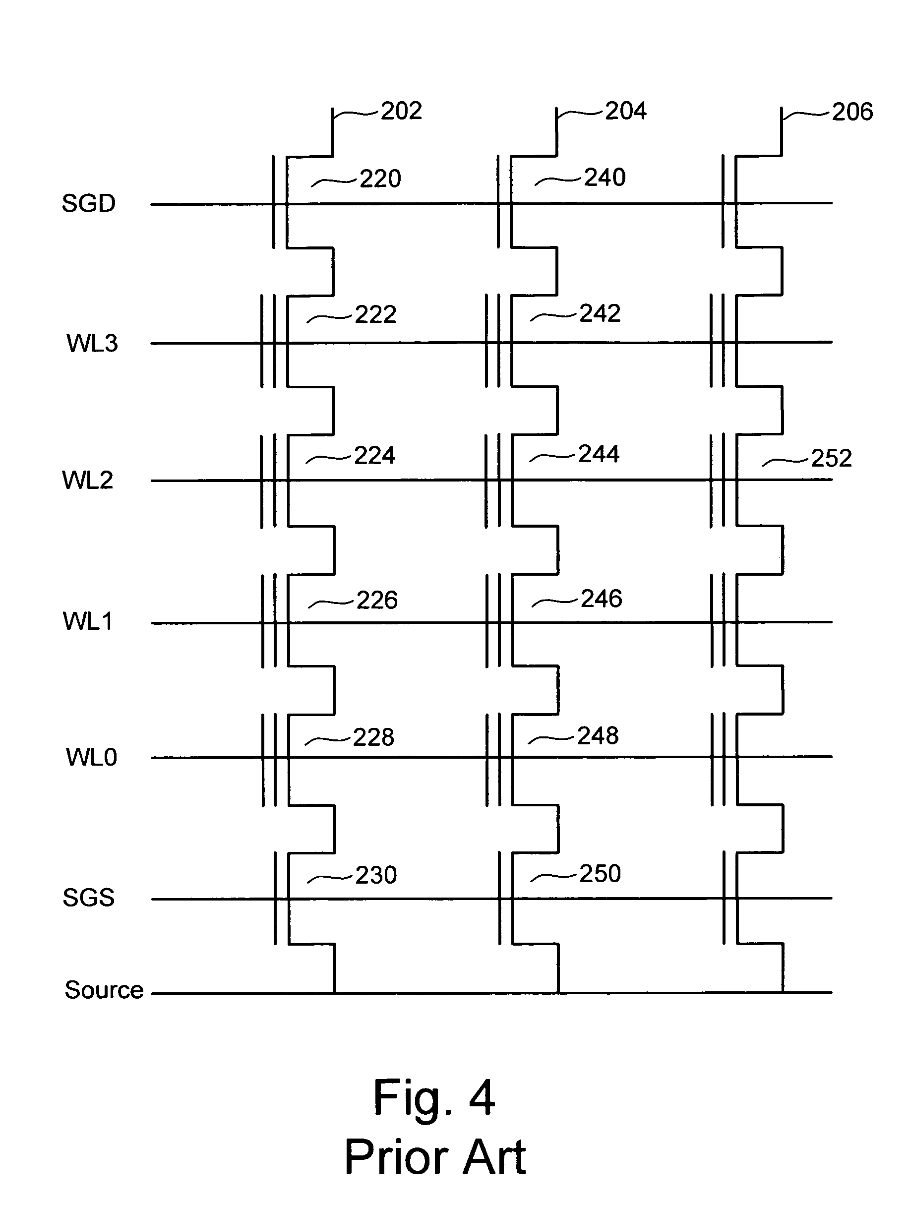
A problem arises when it's desired to program one cell on a word line without programming other cells connected to the same word line, for example, when it's desired to program cell 224 and not cell 244.
Because the program voltage is applied to all cells connected to a word line, an unselected cell (a cell that is not to be programmed) on the word line, especially a cell adjacent to the cell selected for programming may become inadvertently programmed.
Because of this negative charge on the floating gates, the boosting potential doesn't get high enough and there still may be program disturb on the last few word lines.
While these schemes provide an improvement to reduce the occurrence of program disturb, they may not completely eliminate its occurrence and may introduce other problems that can lead to program disturb.

Method used


Image

  • Variable programming of non-volatile memory
  • Variable programming of non-volatile memory
  • Variable programming of non-volatile memory

Examples


Embodiment Construction

[0038]The invention is illustrated by way of example and not by way of limitation in the figures of the accompanying drawings in which like references indicate similar elements. It should be noted that references to an or one embodiment in this disclosure are not necessarily to the same embodiment, and such references mean at least one.

[0039]In the following description, various aspects of the present invention will be described. However, it will be apparent to those skilled in the art that the present invention may be practiced with only some or all aspects of the present disclosure. For purposes of explanation, specific numbers, materials, and configurations are set forth in order to provide a thorough understanding of the present invention. However, it will be apparent to one skilled in the art that the present invention may be practiced without the specific details. In other instances, well-known features are omitted or simplified in order not to obscure the present invention.

[0...


PUM


Abstract

Systems and methods in accordance with various embodiments can provide for reduced program disturb in non-volatile semiconductor memory. In one embodiment, select memory cells such as those connected to a last word line of a NAND string are programmed using one or more program verify levels or voltages that are different than a corresponding level used to program other cells or word lines. One exemplary embodiment includes using a lower threshold voltage verify level for select physical states when programming the last word line to be programmed for a string during a program operation. Another embodiment includes applying a lower program voltage to program memory cells of the last word line to select physical states. Additional read levels are established for reading the states programmed using lower verify levels in some exemplary implementations. A second program voltage step size that is larger than a nominal step size is used in one embodiment when programming select memory cells or word lines, such as the last word line to be programmed for a NAND string.

Description

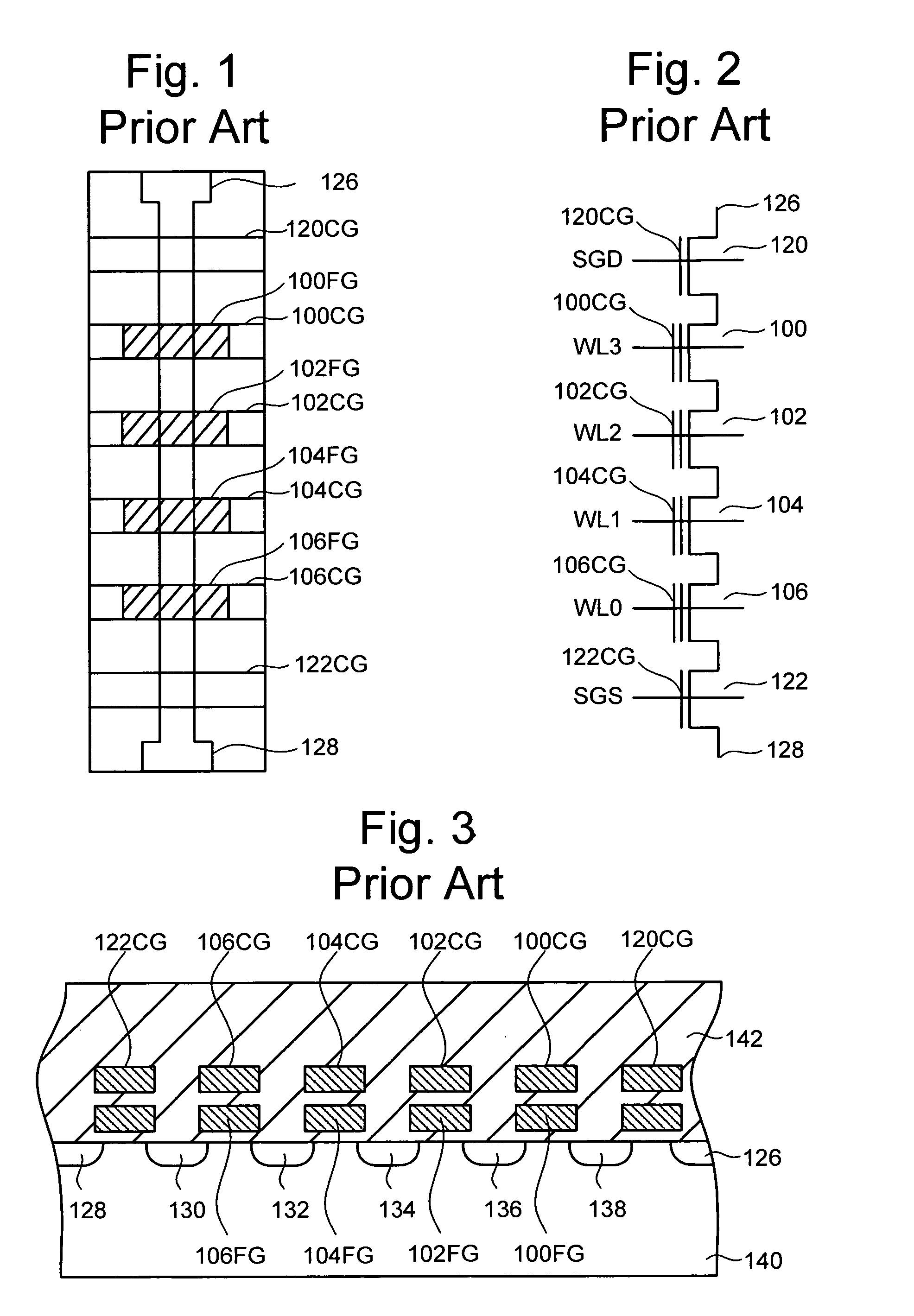
BACKGROUND OF THE INVENTION[0001]1. Field of the Invention[0002]The present invention relates generally to technology for programming non-volatile memory devices.[0003]2. Description of the Related Art[0004]Semiconductor memory devices have become more popular for use in various electronic devices. For example, non-volatile semiconductor memory is used in cellular telephones, digital cameras, personal digital assistants, mobile computing devices, non-mobile computing devices and other devices. Electrical Erasable Programmable Read Only Memory (EEPROM) and flash memory are among the most popular non-volatile semiconductor memories.[0005]One example of a flash memory system uses the NAND structure, which includes arranging multiple transistors in series, sandwiched between two select gates. The transistors in series and the select gates are referred to as a NAND string. FIG. 1 is a top view showing one NAND string. FIG. 2 is an equivalent circuit thereof. The NAND string depicted in F...

Claims


Application Information

Patent Timeline
Patent Type & Authority Patents(United States)
IPC IPC(8): G11C16/04G11C16/34
CPCG11C16/3459G11C11/5628G11C16/3454G11C16/0483G11C16/3418G11C16/3427G11C11/5642G11C2211/5621
Inventor CHEN, JIANWANG, CHI-MING
Owner SANDISK TECH LLC
Learn More