
Mounting power handling components on printed circuit boards near high density routing channels

a technology of power handling components and printed circuit boards, which is applied in the direction of non-printed jumper connection addition, liquid/fluent solid measurement, instruments, etc., can solve the problems of reducing the possibility of placing point-of-use regulators close, wasting a considerable amount of otherwise usable pcb surface area, and reducing the design challenge. achieve the effect of facilitating the distribution of power to the processor

Active Publication Date: 2006-03-28
SANMINA-SCI CORPORATION
View PDF10 Cites 5 Cited by
  • Summary
  • Abstract
  • Description
  • Claims
  • Application Information

AI Technical Summary

Benefits of technology

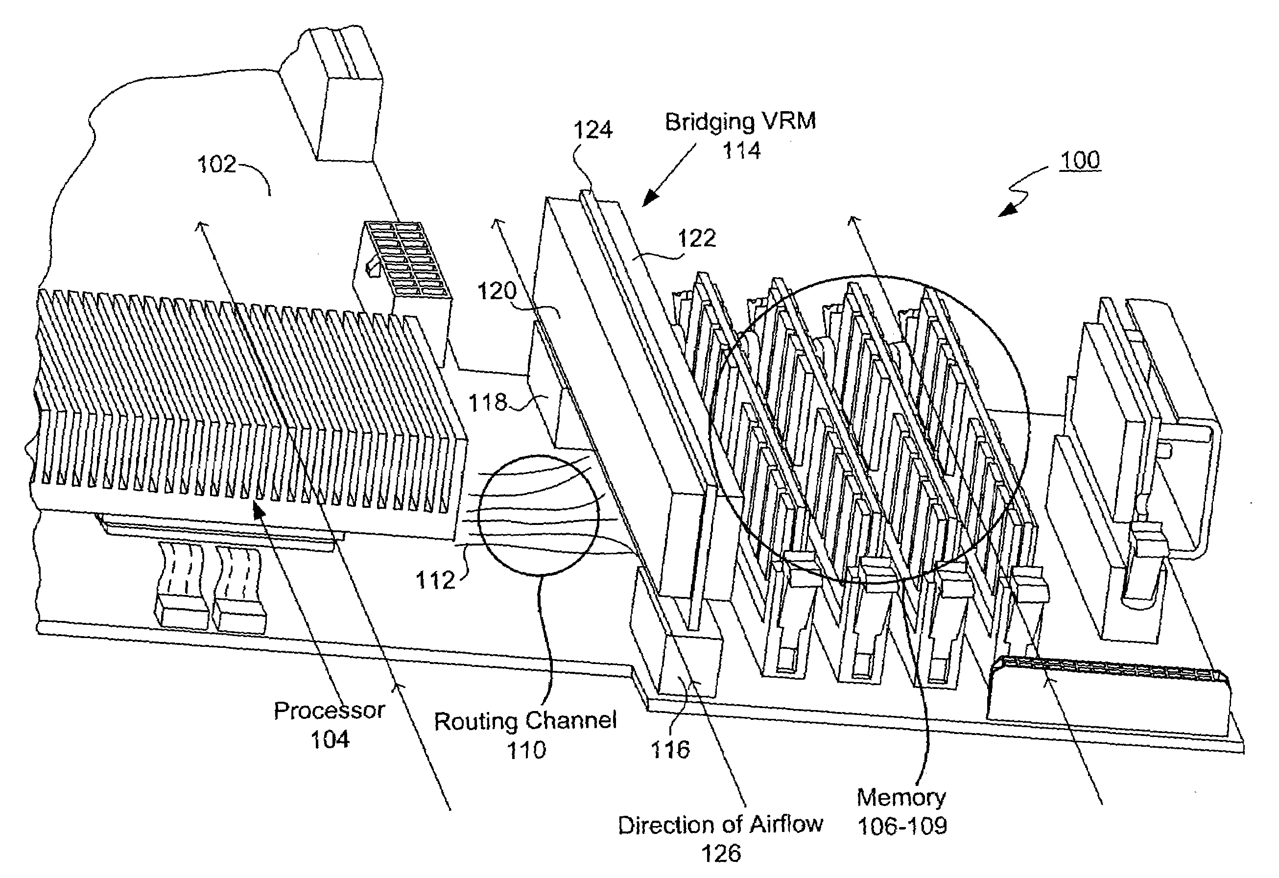
[0007]According to the present invention, techniques are provided by which power handling components may be mounted on PCBs in the vicinity of high density routing channels. According to one embodiment, the invention provides an electronic assembly which includes a printed circuit board, and a processor and a memory mounted on the printed circuit board. A routing channel is provided in the printed circuit board comprising a plurality of conductors interconnecting the processor and the memory. A regulator assembly includes a regulator for providing power to the processor, a first connector mounted on the printed circuit board adjacent a first edge of the routing channel, and a second connector mounted on the printed circuit board adjacent a second edge of the routing channel opposite the first edge. The first and second connectors are coupled to the regulator and facilitate distribution of the power to the processor. The regulator and the first and second connectors form a bridge across the routing channel.
[0008]According to another embodiment, an electronic assembly is provided which includes a printed circuit board having a plurality of circuits mounted thereon. A routing channel is provided in the printed circuit board comprising a plurality of conductors for interconnecting the plurality of circuits. A regulator assembly includes a regulator for providing power to at least one of the circuits, a first connector mounted on the printed circuit board adjacent a first edge of the routing channel, and a second connector mounted on the printed circuit board adjacent a second edge of the routing channel opposite the first edge. The first and second connectors are coupled to the regulator and facilitate distribution of the power to the at least one of the circuits. The regulator and the first and second connectors form a bridge across the routing channel.
[0009]According to another embodiment, an printed circuit board assembly is provided which includes a printed circuit board. A routing channel is provided in the printed circuit board comprising a plurality of conductors for interconnecting a plurality of circuits mounted on the printed circuit board. A first connector is mounted on the printed circuit board adjacent a first edge of the routing channel. A second connector is mounted on the printed circuit board adjacent a second edge of the routing channel opposite the first edge. The first and second connectors are configured to be coupled to a regulator and facilitate distribution of power therefrom to at least one of the circuits. The first and second connectors also being configured to form a bridge across the routing channel with the regulator.

Problems solved by technology

This difficult design constraint is made more challenging by the introduction of through-holes and vias for components mounted on the PCB in the region of the routing channels in which the interconnects are disposed.
However, this wastes a considerable amount of otherwise usable PCB surface area.
In addition, such an approach undesirably restricts the options for placing point-of-use regulators close to the components with which high density interconnects are associated.
The disadvantage of such an approach is that it may raise the height profile of the assembly beyond acceptable limits.

Method used


Image

  • Mounting power handling components on printed circuit boards near high density routing channels
  • Mounting power handling components on printed circuit boards near high density routing channels
  • Mounting power handling components on printed circuit boards near high density routing channels

Examples


Embodiment Construction

[0013]Reference will now be made in detail to specific embodiments of the invention including the best modes contemplated by the inventors for carrying out the invention. Examples of these specific embodiments are illustrated in the accompanying drawings. While the invention is described in conjunction with these specific embodiments, it will be understood that it is not intended to limit the invention to the described embodiments. On the contrary, it is intended to cover alternatives, modifications, and equivalents as may be included within the spirit and scope of the invention as defined by the appended claims. In the following description, numerous specific details are set forth in order to provide a thorough understanding of the present invention. The present invention may be practiced without some or all of these specific details.

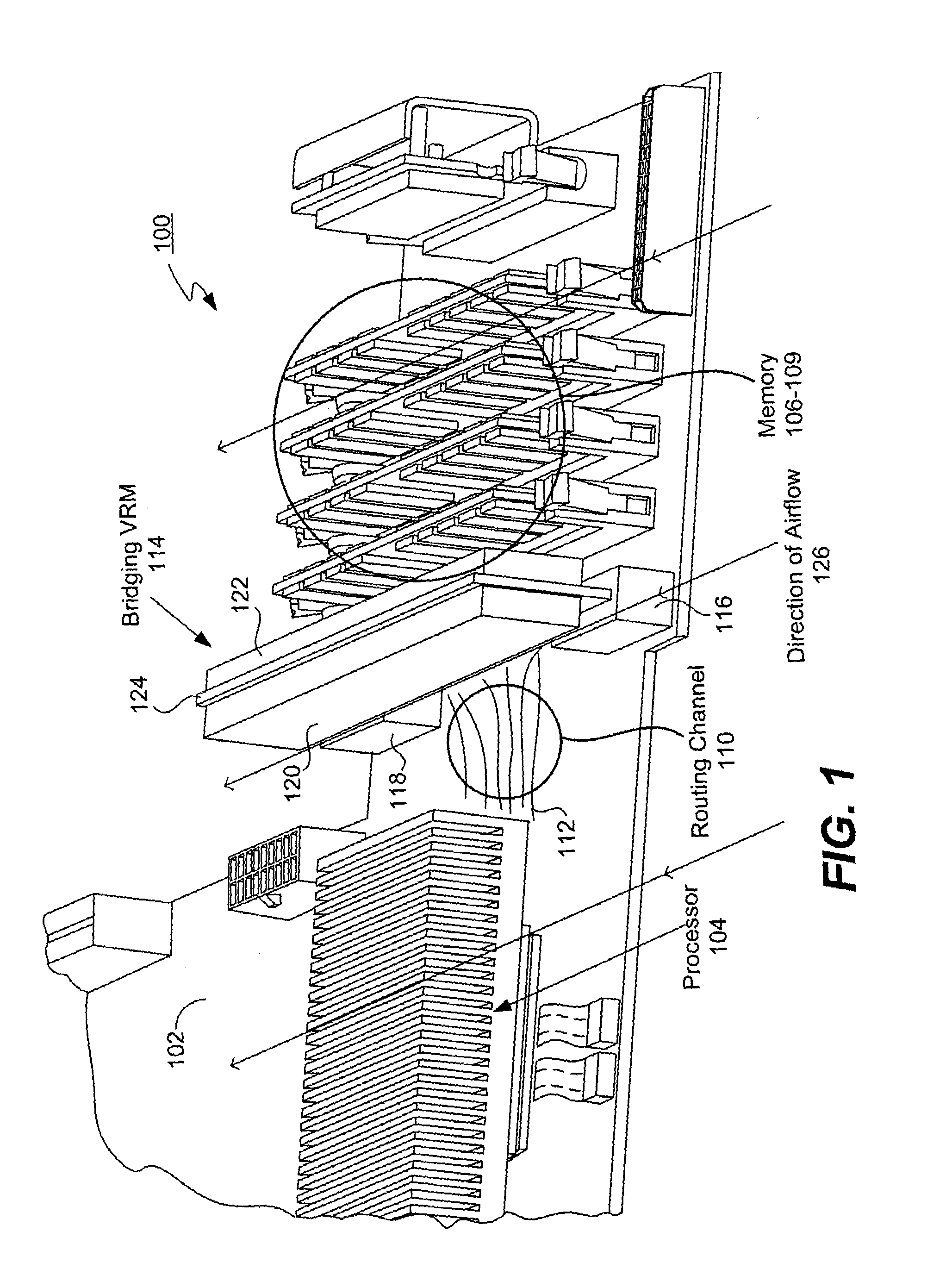
[0014]FIG. 1 is a simplified representation of a portion of a motherboard assembly 100 to facilitate illustration of a specific embodiment of the inve...


PUM


Abstract

An electronic assembly is described which includes a printed circuit board, and a processor and a memory mounted on the printed circuit board. A routing channel is provided in the printed circuit board comprising a plurality of conductors interconnecting the processor and the memory. A regulator assembly includes a regulator for providing power to the processor, a first connector mounted on the printed circuit board adjacent a first edge of the routing channel, and a second connector mounted on the printed circuit board adjacent a second edge of the routing channel opposite the first edge. The first and second connectors are coupled to the regulator and facilitate distribution of the power to the processor. The regulator and the first and second connectors form a bridge across the routing channel.

Description

BACKGROUND OF THE INVENTION[0001]The present invention relates to printed circuit boards and, more specifically, to techniques for mounting power handling components on printed circuit boards in regions corresponding to high density routing channels.[0002]Electronic assemblies constructed on printed circuit boards (PCBs) often employ point-of-use regulators in close proximity to the components to which they provide power for the purpose of reducing noise and power losses. For example, each processor on a computer system motherboard might have its own associated voltage regulator module (VRM).[0003]Recent generations of processor designs have integrated the memory controllers which facilitate communication between the processors and associated memory. As a result, high density interconnects are provided directly between the processors and the memory. Because of the extremely high operational speeds of these processor designs, the dimensions of the conductors in such high density inte...

Claims


Application Information

Patent Timeline
Patent Type & Authority Patents(United States)
IPC IPC(8): H05K7/02H05K7/06H05K7/08H05K7/10G06F1/18G06F1/26H05K1/02H05K1/14H05K3/22H05K3/36
CPCG06F1/189G06F1/26H05K1/141H05K1/0262H05K1/0263H05K2201/10189H05K3/222H05K3/366H05K2201/044H05K2201/09236
Inventor RECORD, LESLIE J.KULPA, WILLIAM G.GONTAREK, ROBERT
Owner SANMINA-SCI CORPORATION
Learn More